Authored by Ruben Medina
E-mail: medina72@unlv.nevada.edu
Date: 11/1/2013
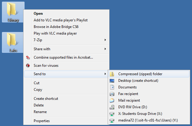
To start the pre-lab I backed up my library and lab files to Dropbox:
Next, I went through Tutorial 5 located here.
Then, for the last part of the pre-lab I read through the lab before I started it.
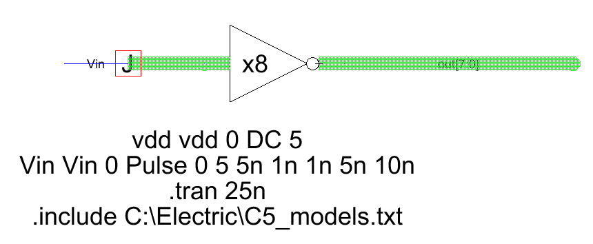
For the first part of the lab, I created an 8-bit inverter by placing the icon of the 1-bit inverter in a new schematic and naming it (with q) inverter[0:7].
Then I added buses and off-page nodes for the input and output with 8-bit labels and created an icon.
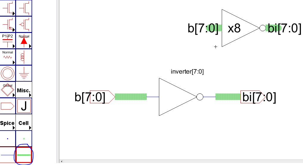
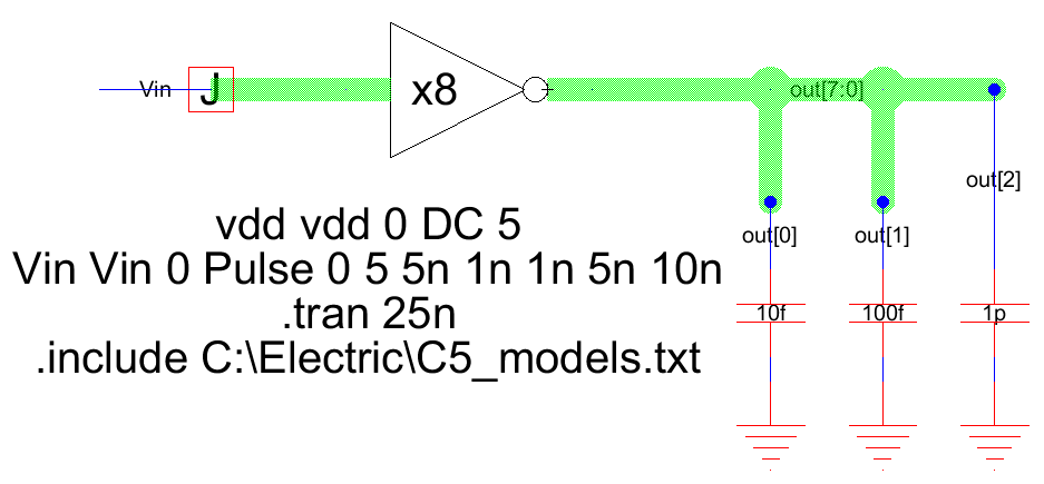
Next, I created a simulation schematic for this new 8-bit inverter by making a new schematic and using the icon I just created.
Note, the boxed J is a wire-con component which joins the bus together into a single wire. I also gave the output an 8-bit label.
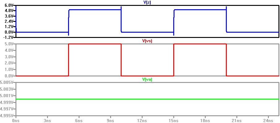
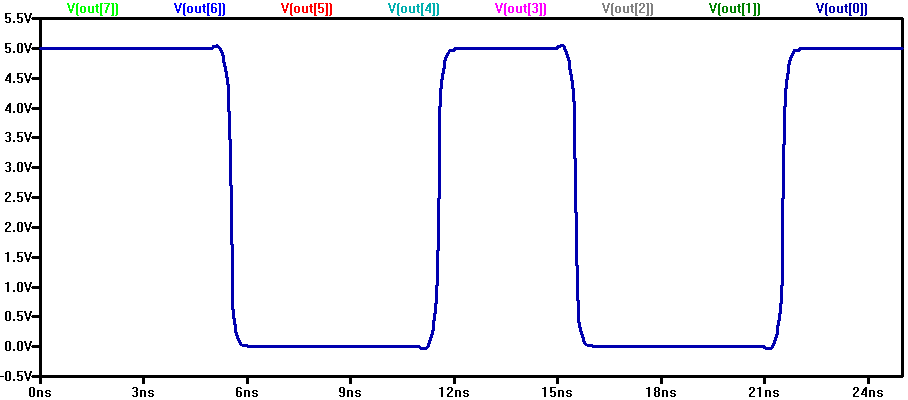
I then ran LTSpice for the simulation of the schematic:
Next, I added various capacitances to the simulation schematic in order to see how they would effect the operation of the circuit:
I then ran an LTspice simulation on the schematic:
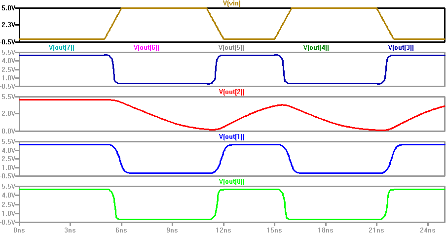
We can see that as the capacitance goes up, the inverter begins to not operate correctly and the output is distorted.
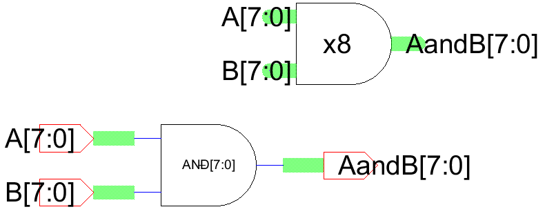
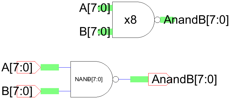
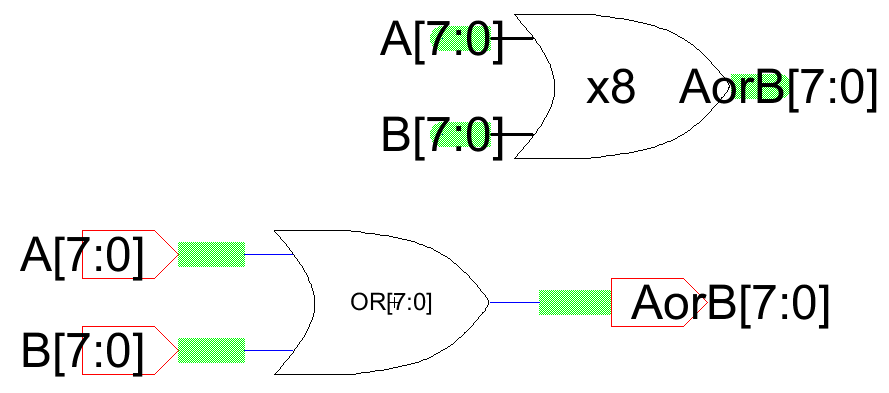
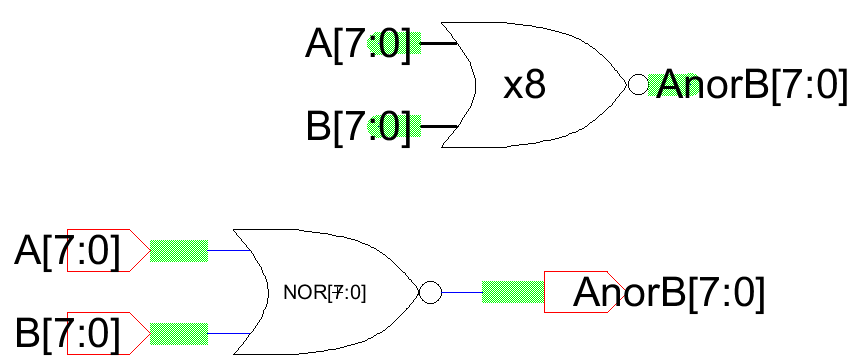
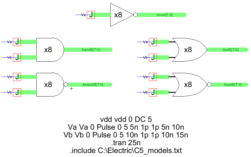
For the next part of the lab, I created schematics and icons for 8-bit input/output AND/NAND/OR/NOR gates.
The AND gate can be seen below:
The NAND gate can be seen below:
The OR gate can be seen below:
Finally, the NOR gate can be seen below:
To simulate all of these new gates, I created a new simulation cell and added the icons for the inverter, AND, NAND, OR and NOR:
The resulting simulation can be seen below:
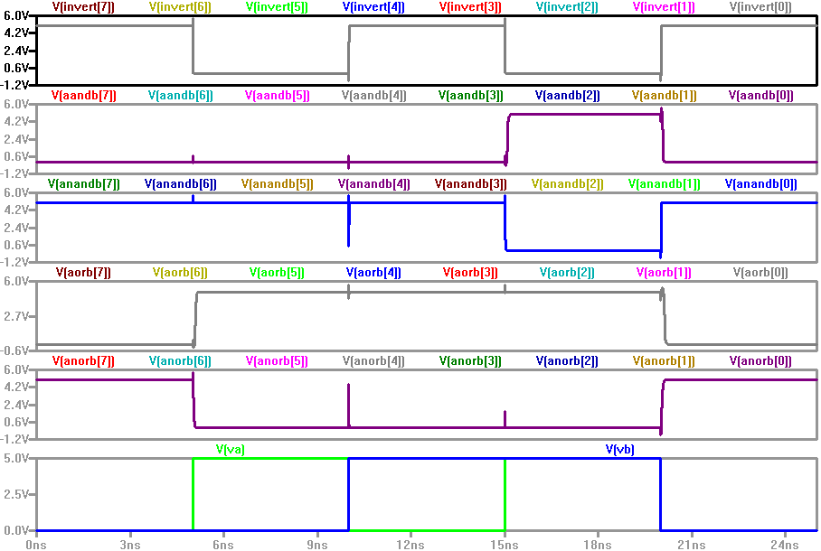
We can see that each gate is operating correctly and that with a single input for each gate, the 8-bit output is consistent for all of them.
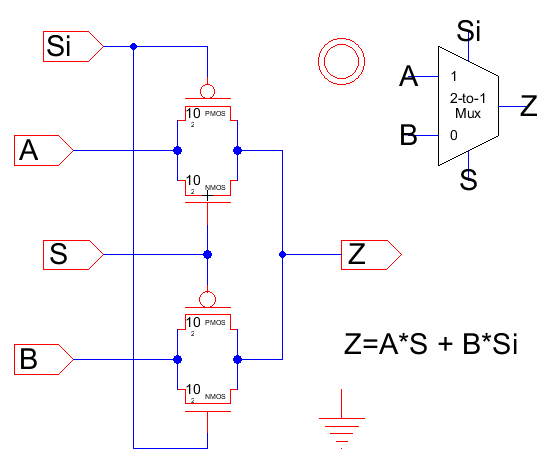
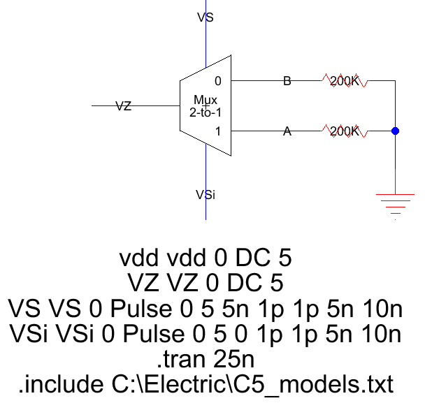
Next, I created the schematic and icon for a 2-to-1 multiplexer:
I then made a simulation schematic using this icon and ran the spice code simulation in LTspice:
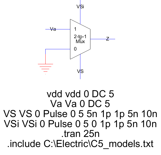
Simulation:
We can see that with one input grounded and the other tied high, when the high input is selected, the output matches the select signal.
In more detail, looking at the schematic we see that when S is high (and Si is low) one set of PMOS and NMOS is ON allowing the A signal to pass. When S is low (Si high) the other set of PMOS and NMOS is ON, passing the B signal.
The 2-to-1 multiplexer can be used as a 1-to-2 de-multiplexer by turning it around and making the Z signal the input.
However, when checking via simulation the correct output of A and B could only be achieved when they are tied to pull-down resistors. This can be seen in the simulation schematic below:
The LTspice simulation:
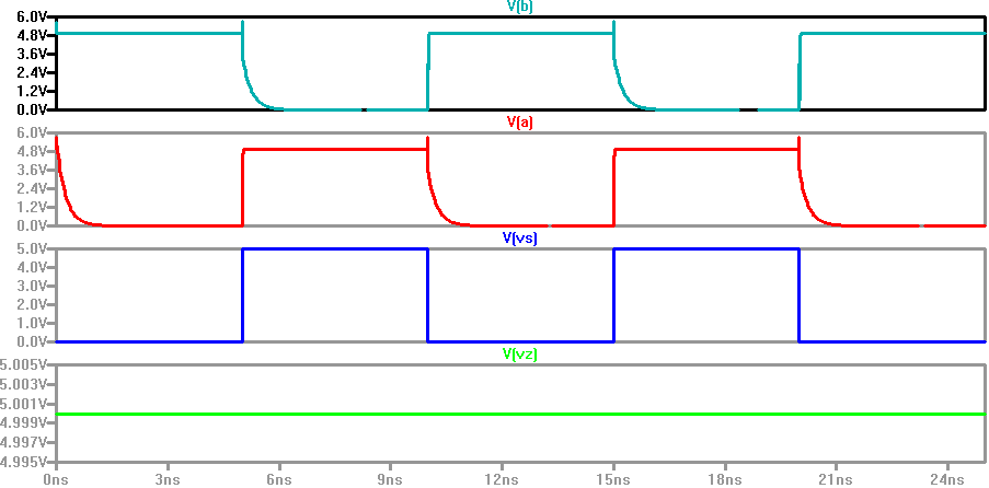
Without adding the pull-down resistors, the output voltages do not return to 0 during simulation.
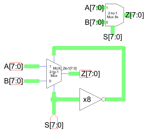
Then, I created an 8-bit multiplexer schematic and icon and included the previously made 8-bit inverter in order to only need 1 select input signal.
Then, in order to verify the operation of the schematic, I created a simulation schematic cell:
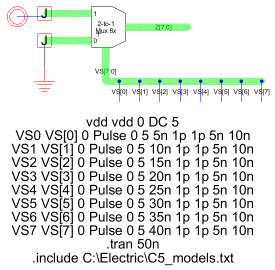
The LTspice simulation can be seen below:
We can see for each bit of the multiplexer, as its select signal is enabled each bits output signal follows the select signal due to the input voltages being tied to high and ground.
The IRSIM for the schematic using the command file located here:
Again we can see that each bits output signal is the same as its select signal similar to the LTspice simulation.
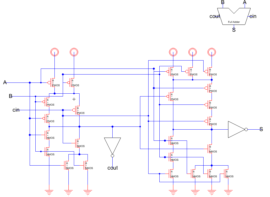
Next, I drafted the schematic and icon for the full-adder seen in Fig. 12.20 of the book using 6/2 NMOS/PMOS devices:
Then, knowing that the next step was to create an 8-bit full-adder, I drafted the layout for this 1-bit schematic:
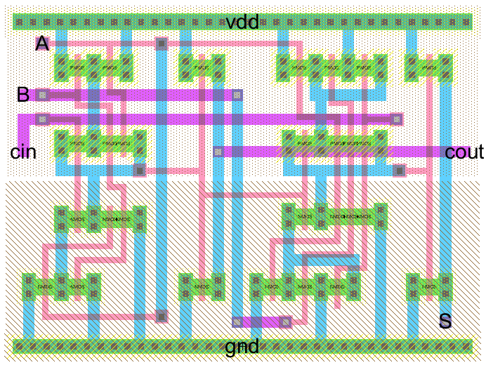
I then ran well, DRC, and LVS checks on this layout:
I then ran a quick IRSIM using the command file located here from the previous lab:
We can see that the 1-bit full-adder is working correctly.
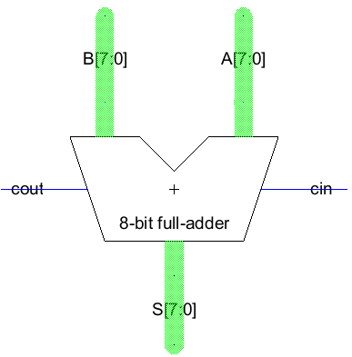
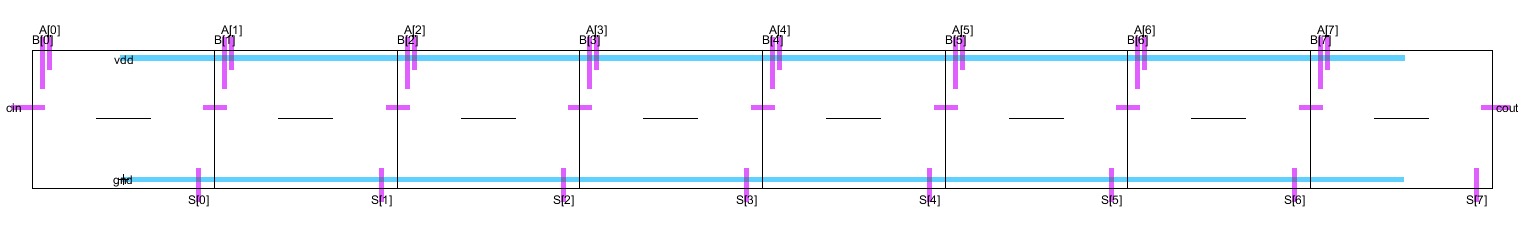
Finally, I drafted the schematic and icon for an 8-bit full-adder using the icon of the previously made 1-bit full-adder and buses:
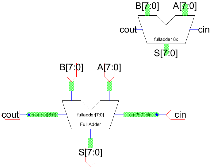
Note that the array of adders goes from 7 to 0 so the first adder from left to right is adder[7] and its cout is the export cout, adder[6]'s cout is out[6], etc. Also, adder[0]'s cin is the export cin, adder[1]'s cin is out[0], etc.
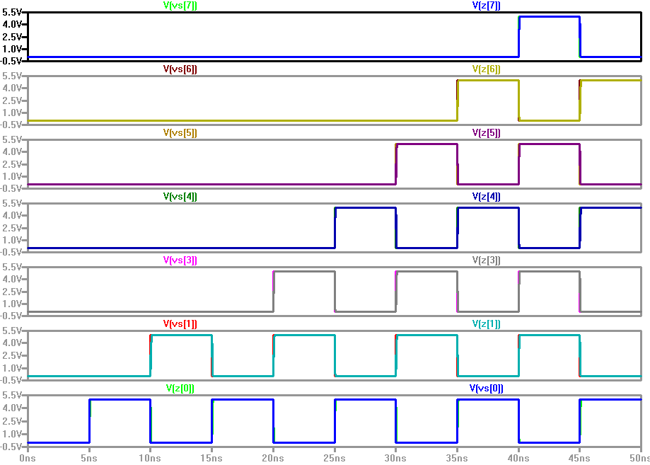
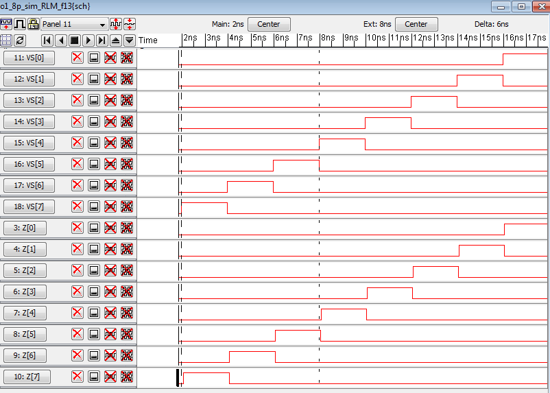
Next, I created a simulation schematic for this 8-bit adder:
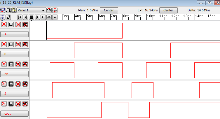
And then ran an IRSIM simulation:
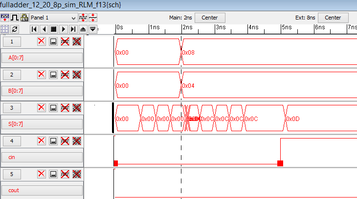
We can see that the output is correct for the 8-bit input words set by the simulation file located here.
With the simulation confirming the correct operation of the 8-bit adder I then moved on to drafting the layout
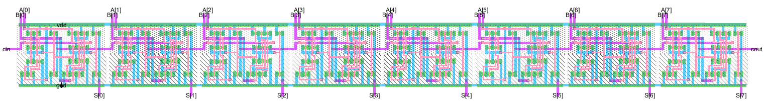
I drafted the layout by dragging the layout of the 1-bit adder into the 8-bit adder layout and copying six times and then adding the required cout->cin connections as well as the appropriate exports for inputs and outputs:
Opened to show complete layout:
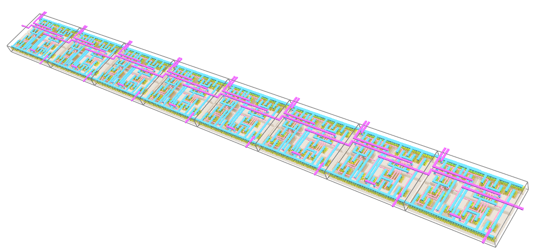
And finally, the 3d view:
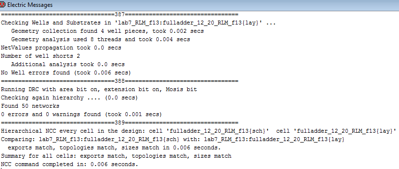
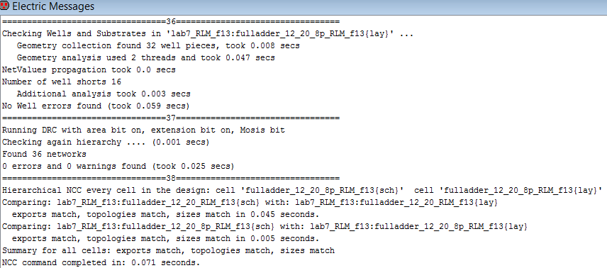
To complete the layout I then ran well, DRC, and LVS design checks:
My completed schematics, icons, and full-adder layouts can be found in my lab 7 jelib located here.
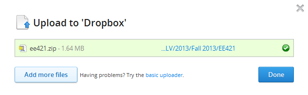
To finish the lab, I again zipped my library and lab folders and uploaded the resulting zip file to Dropbox: