Lab 5 - ECE 421L
Authored
by Michael Kajkowski,
10/4/2013
kajkowsk@unlv.nevada.edu
For this lab we will be learning how to make an inverter using nmos & pmos transistors.
We will be designing these inverters in schematic, icon, & layout cells.
Additionally, we will be learning how to add a multiplier to the transistors.
Finally, we will simulate our inverter using Spice, ALS, & IRSIM.
The first we will design a 20/10 inverter( where the nmos has 10/2 & pmos has 20/2), next we will
design a 100/50 inverter (where the nmos is 20/2 with a M=5 multiplier, making it 100/2 & the pmos
is 10/2 with a M=5 multiplier, making it 50/2).
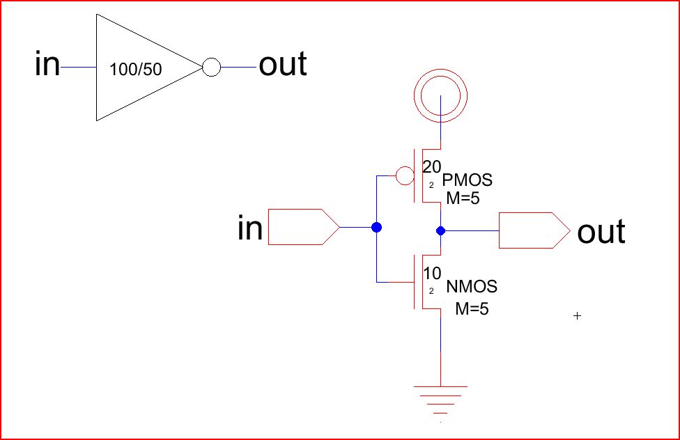
Making the schematic:
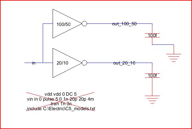
Lets start by starting Electric and opening a new schematic cell. Place a pmos and nmos transistor
in the cell. Click on the transistors and goto Tools->Simulation(Spice)->Set Spice Model. Change the text
to NMOS for the nmos transistor and PMOS for the pmos transistor. For the pmos, you will set the width=20 and length=2.
For the nmos, you will set the width=10 and length=2. The following schematic shows you what your schematic should
look like....

Make sure you export (ctrl E) your terminals in and out. After you created your inverter, you will make an icon.
This is the same process as done in previous labs, all you need is a triangle, from the components list and a circle.
You want to reduce the size of the circle. Notice the 20/10 inverter icon seen above.
Making the layout:
Open a new layout cell. Make sure to name it the same as your schematic. Create the pmo and nmos transistors
the same way as done in the last lab. Be sure to use the same width and length as the schematic transistors.
Your layout should look like this....
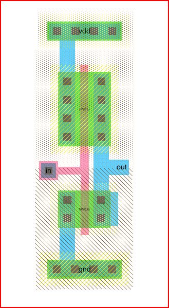
Notice that the p-well connects the nmos bulk to ground (export as gnd), and
the n-well connects the pmos bulk to VDD( export as vdd). Export the in and out.
Also, apply set spice model to the transistors (NMOS/PMOS).
Be sure to connect the poly's with poly arc (the pink) and all other contacts with metal 1 (blue).
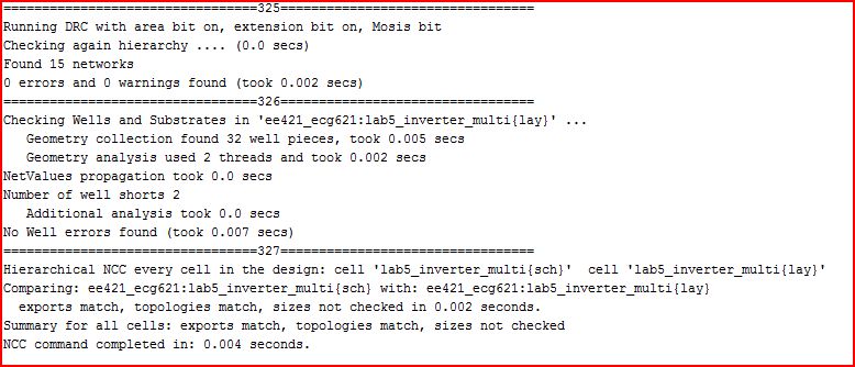
Make sure you perform DRC, ERC and NCC check. Note, it is very useful to do these checks bit by bit.
This way if there is an error you can pin point where extactly your problem is. You will have to play with the
arc characteristics (end extensions), by ctrl I the arcs.
Schematic & Layout for multiplier:
This
process is very similar to the 20/10 inverter. Except in the schematic
you will click on the transistors and goto
Tools-> Simulation(Spice)-> Add Multipier. You will see M=1 appear on the transistor. Change it to M=5 for both the
nmos and pmos. Making the icon is exactly the same process. The schematic should look like this...
The
layout is a little more difficult. Duplicate the previous layout. Make
an array 5 times horizontally, for the pmos and nmos.
Remember
that the number of poly's is the number of transistors. These
transistors will be connected in parallel. Where the total
width will be multiplied by the number of poly's and the length will remain the same. Hence, we will be making a 100/50 inverter.
Next, get rid of the contacts on the left side of each transistor. Then, connect the pmos transistors side by side using select.
Same for the nmos. You can now move the transistors closer together. Remember to do a well check often and DRC. The
layout below shows you what connects need to be made....
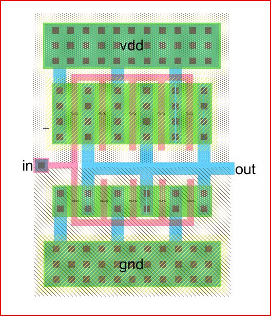
Remember to export your terminals and do NCC. Also, you will want to make adjustments on the end extension
arc characteristics.
Here is my DRC, ERC, and NCC....
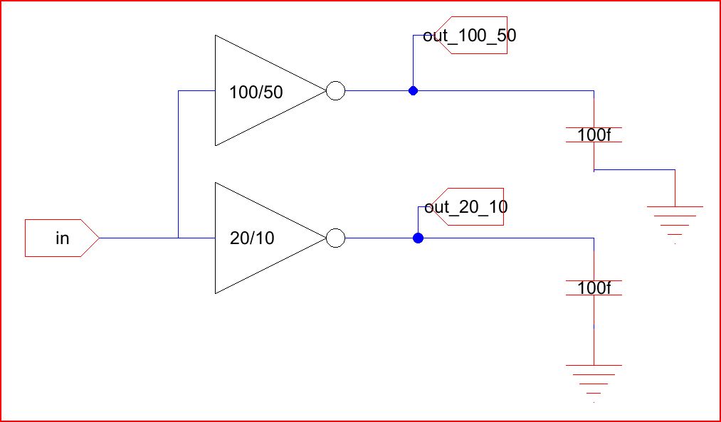
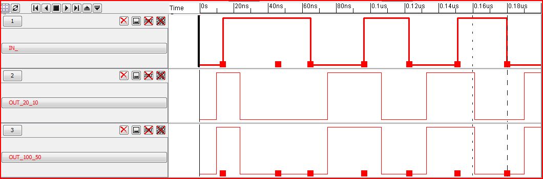
Spice Simulations:
100fF Load:
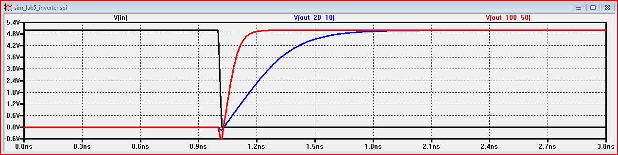
The 100/50 has a smaller time delay then the 20/10. The increased width makes it more suitable for
digital switching because its transitions much more faster.
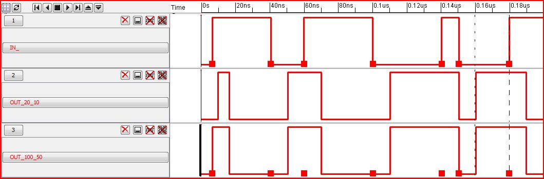
1pF Load:

Notice how the time delay has increased by approximately 2ns.
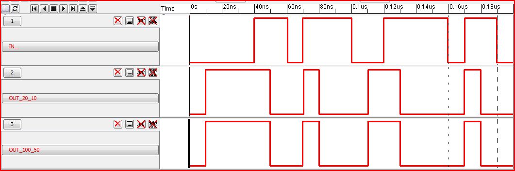
10pF Load:
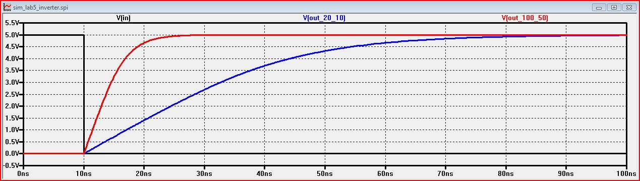
The time delay has increased more.
Each load had an increased by a factor of roughly 10.
ALS Simulations:
For the ALS sim you will need to use these off page nodes and export them. Goto Tool-> Simulation(Built-in)->ALS
100fF:
Appears to be no difference in delay between the two inverters.
1pF:
The time delay appears to be the same.
10pF:
No difference in inverters. The delay appears to be the same, a time delay roughly 10ns.
The ALS is strictly a logic simulator. It is not as detailed as the Spice simulator. Also,
it seems like the change in load was the same, or at least close, between the two inverters.
Also, the change in time delay appears to not change with different loads.
IRSIM Simulations:
100fF:

1pF:
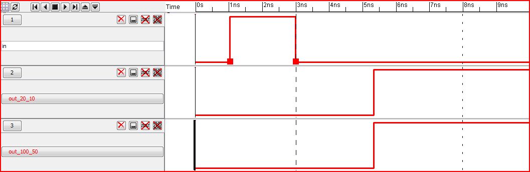
The time delay had greatly increased.
10pF:


As you can see the delay increased much more. The input went high around 1ns and the outputs responded
around 29ns.
As stated before, ALS is a logic simulator (and we have seen it's limitations compared to spice) and is more suited for
transistor level design. The IRSIM sim does model transistors, which is useful for digital design.
REMEMBER TO SAVE AND BACKUP ALL OF YOUR WORK!!!
My jelib file
Return to Labs