Lab 4 - ECE 421L
Authored
by Michael Kajkowski,
Today's Date: 9/26/2013
Email: kajkowsk@unlv.nevada.edu
For this lab we will be learning how to design NMOS & PMOS transistors.
We will go over the procedure for creating MOSFET's in schematic, layout, and icon cells.
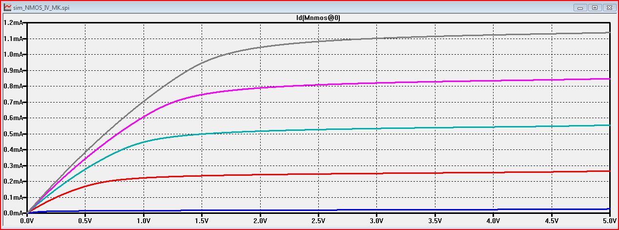
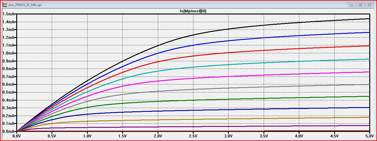
Additionally, we will simulate our schematics to demonstrate the I-V characteristics.
Before we start, remember to save and back up all of your previous work!
Also, be sure to download C5_models.txt.
Creating the NMOS schematic:
1. Start Electric and open a new schematic cell called "NMOS_IV". You can add your
initials to it. (e.g. NMOS_IV_MK).
2.Select the NMOS part from the components list (indicated by the blue circle below).
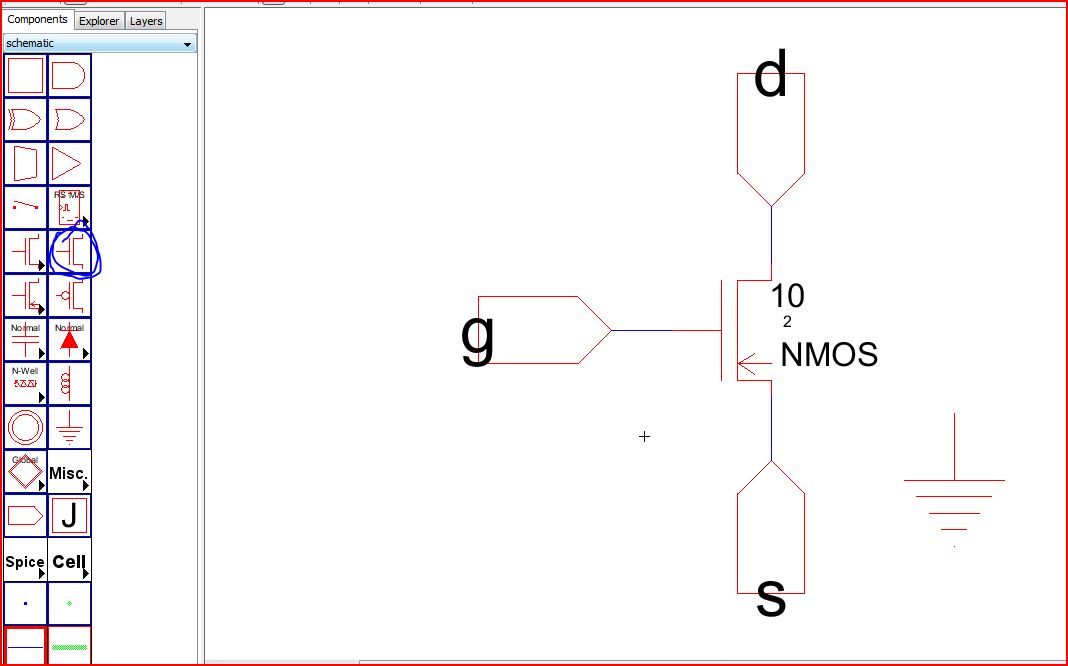
3. Select the NMOS symbol and ctrl I. Change the NMOS size to width=10 and length=2.
4.While the symbol is still selected, goto Tool -> Simulation (Spice) -> Set Spice Model.
Spice text should appear over the NMOS symbol. Change the text name to NMOS.
5. Place a ground in the schematic. (Note that if using a 3 port NMOS transistor you will not need to
connect the ground, but you will need to connect the ground to bulk for a 4 port transistor).
6. Export (ctrl E) the terminals of the NMOS d,g,s.
7. (Optional) If you wanted to be able to connect the bulk/body of the NMOS/PMOS, you will
need to use a 4 port transistor. Select the transistor symbol and goto to Edit -> Change (or just hit C).
A window will appear and you will be able to select the for 4 port transistor as seen below...
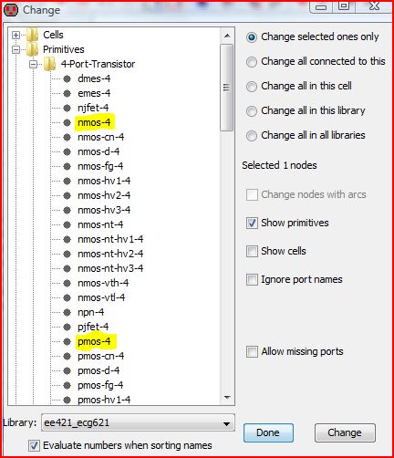
Select nmos-4 for NMOS and pmos-4 for PMOS.
Creating the NMOS Layout:
1. Open a layout cell and name it the same as the schematic.
2. From the mocmos component list select the NMOS and place in the layout.
3. Select it and change the width to 10 and the length to 2.
4. While the NMOS is still selected, goto Tools -> Simulation (Spice) -> Set Spice Model.
5. New text will appear over the NMOS symbol. Change the text to NMOS.
6. Place two NAct parts on the layout, one above and one below the NMOS. Change their
widths to 10.
7. Place the Metal1-Polysilicon (purple/pink box) on the left of the NMOS, it should slightly overlap.
8. Place P-well node on the layout, the width should be 10 (this will connect to ground).
9. Connect the top nAct to the top port of the NMOS, and connect the bottom nAct to the bottom port of the NMOS.
(Remember to left click - right click to make the connections with arcs, also change the arc widths to 5).
10. Once the nActs are connected, move them as close as possible to the NMOS without ERC errors.
11. Move the P-well node at the bottom of the device, it should overlap the substrate.
12. Select the Metal1-Poly connector and connect to the poly ( the bar that goes across the NMOS active region)
with metal 1.
13. Your layout should look like this....
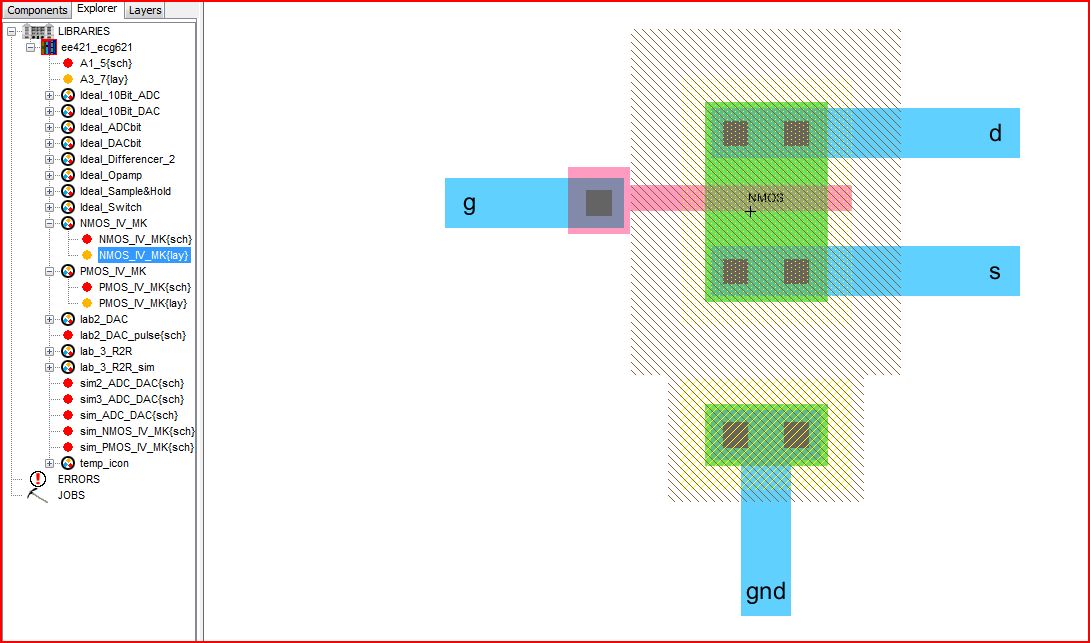
14. Add metal 1 the terminals as seen above. Export the metal1 nodes as g, d, s, gnd.
15. Perform a ERC well check in the layout view, DRC in the schematic, and NCC check.

Creating an Icon:
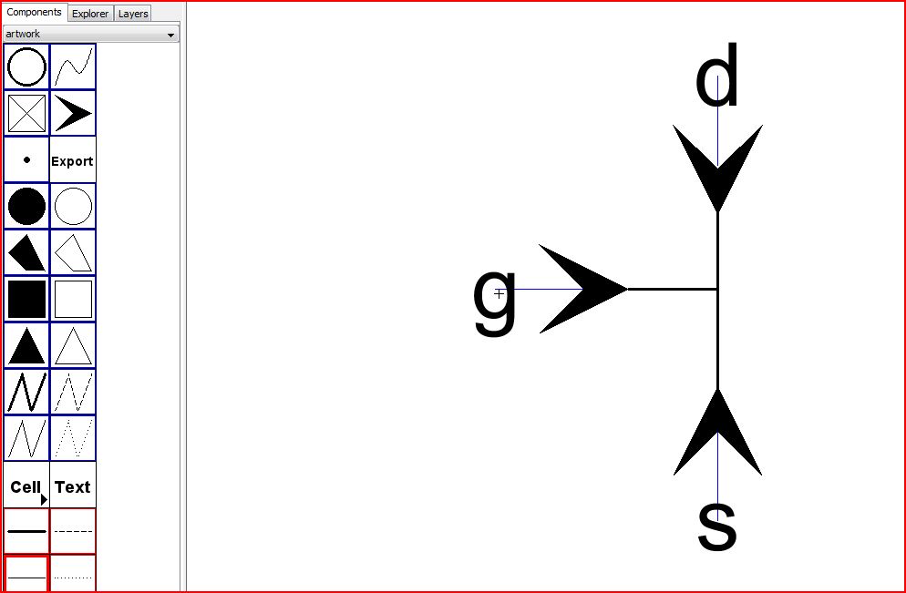
Goto
your schematic view, goto View -> Make Icon View. As done before
from previous labs, goto your new ic cell (which should
have the same name as your schematic) and using different shapes and lines, create your own symbol. Be sure
to label your terminals they same way in the schematic. Here is an example of an NMOS icon...
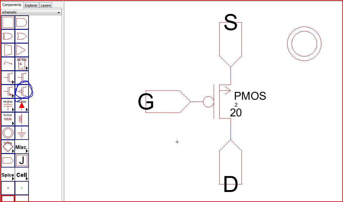
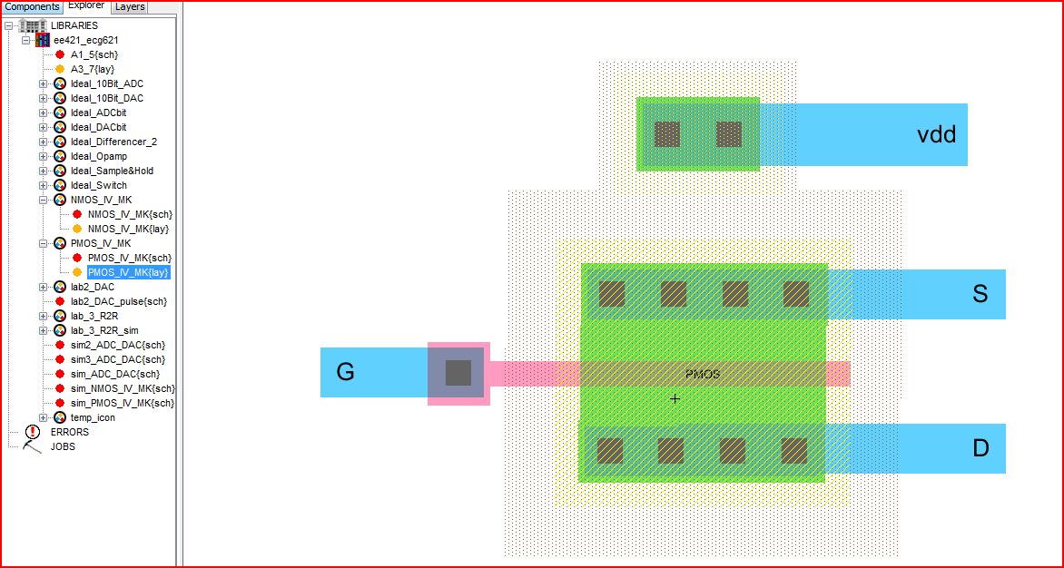
Creating the PMOS schematic:
Follow the same steps as the NMOS except here are some differences:
1. Use PMOS, instead of NMOS (naming, spice modeling, selection of the transistors for schematic and layout.)
2. Set the width of the transistor to 20 (This is due to differences in mobility).
3. Use n well's instead of p well's.
4. Use pActs instead of nActs.
5. In the schematic, instead of placing a ground for the NMOS, place a power node (the circle from components).
6. The bulk/body will be connected to VDD instead of ground.
7. Besure to perform DRC, ERC, & NCC checks.
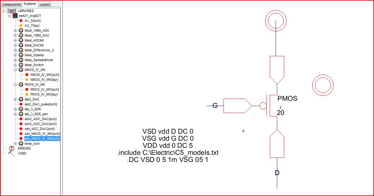
Your schematic & layout should look like this....
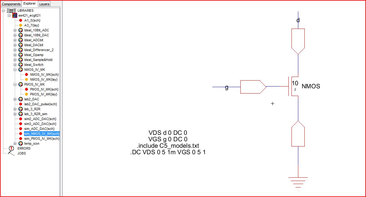
Creating the simulations:
1. Duplicate your NMOS & PMOS schematic cells and name them "sim_NMOS_IV" and "sim_PMOS_IV".
2. For these schematics you will not need to export the terminals. Just label them using crtl I.
3.From the components list, add spice code (from misc.) to your two new schematic cells.
Here is what your schematics and simulations should look it (use the spice code as seen below)...
REMEMBER TO BACKUP ALL OF YOUR WORK (CREATE ZIP & EMAIL TO YOURSELF)!!!
Return to Labs