Lab 3 - ECE 421L
Authored
by Michael Kajkowski,
Today's
date is 9-20-2013
Email: kajkowsk@unlv.nevada.edu
Lab
description:
For this lab we will be preforming the same lab as last time, except this time we will be
laying out n-well resistors to create the R2R circuit. This process will consist of creating
a layout and laying out the R2R with the n-well, creating the R2R schematic, creating an icon, performing the
DRC, ERC, & NCC checks and finally running the ADC-DAC simulation.
Create the layout:
From the component list, select N-RWell part and place it on the layout. This is the resistor you will use.
Select the width to be 15 (lambda) (min. needs to be 12). We know that the R/square is 800. We can determine the
length that we need to get our 10K resistor. 10k=800(length/15) -> length is 187.5.
Now lets copy this resistor twice. Connect the three resistors using metal 1. Note that there is
a minimum space requirement between the N-Rwell parts. You will want to play around with the spacing
and periodically perform an ERC (well check). The layout should look like this...

Note that it is optional to surround the resistors with p-active. Next, be sure to export the
three terminals as seen above.
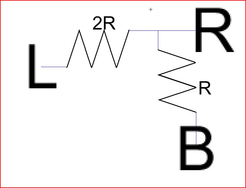
Creating the icon:
Next we will create the R2R icon. This step is simple to do. Click View-> Make icon view. A box should
appear with the generated icon, with the terminals for L,R, and B. In the component list you can select shapes
to create your own icon. For this it would be best to use line segments to imitate resistors.
Creating the schematic:
Create a new cell. It will be a schematic cell. Here you will basically drag your new icon into this cell.
And make 9 copies of it. You will connect them up the same way you did in the previous lab.
It should look like this...

Be sure that export the output/input labels (B0, B1, Vout, etc.)
Perform the ERC, NCC, and DRC checks:
Goto the Tools tab and yo will see options for ERC, DRC, and NCC.
The DRC will check your schematic for any bad connections or
extra pins, etc. The ERC will check your wells on your layout.
The NCC will that your schematic layout match up.
Here's an example of an ERC check...

Running a simulation:
The final thing to is verify that my R2R layout circuit works. For this step
I created a new sim3_ADC_DAC file (it contains the DAC_ADC circuit).
I also created a new DAC icon for my R2R schematic. After this I replaced
the old DAC with the new one (In the sim3 file).
The simulations looks like this...
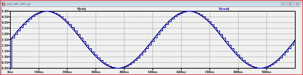
As you can see the simulation reveals that my layout was successful!
REMEMBER TO BACKUP ALL OF YOUR WORK (CREATE ZIP & EMAIL TO YOURSELF)!!!
Here is a link to my jelib file: ee421_ecg621.jelib
Return to Labs