 Lab 8 – EE 420L
Authored by: Daniel Senda
Email: sendad1@unlv.nevada.edu
Spring 2019
Due: 04-10-2019
1) Introduction
This lab
introduces students to the process of characterizing MOSFETs using experimental
data. In addition, it also goes over inverter delays and the process to
characterize that too.
2) Pre-Lab Description
This pre-lab
required the student to complete the following before proceeding with the lab:
- Read the datasheet of the CMOS Dual
Complementary Pair Plus Inverter chip (CD4007) and
become familiar with it.
- Understand how the bodies of the NMOS
devices are connected to VSS (typically GND or the lowest potential in the circuit)
and how the bodies of the PMOS devices are connected to VDD (typically 5V or
the highest potential in the circuit). Also, note that VSS is pin 7 and that
VDD is pin 14 on the chip.
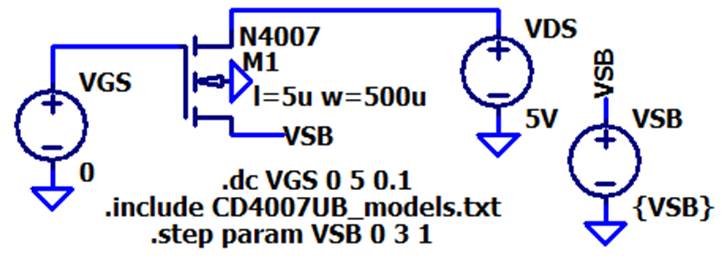
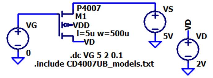
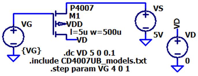
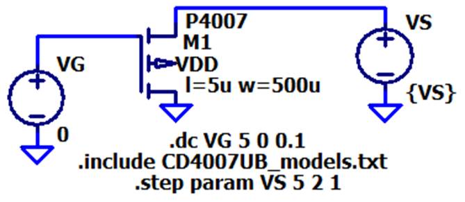
3) Description of Lab
Procedures
This lab
instructs the student to utilize the CD4007 chip and
not the CD4007UB chip. Due to no availability of the
CD4007 chip, the professor let the students utilize the CD4007UB chip instead.
The student was instructed to assume that the MOSFETs used in this lab will be
powered by a +5V power supply. Furthermore, the devices should not be
characterized at higher than +5V or lower than 0V ground potential.
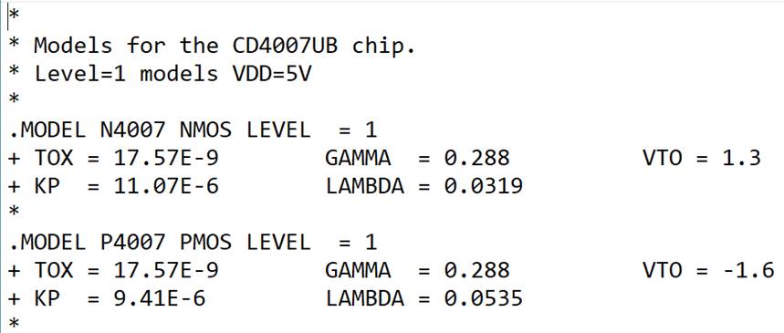
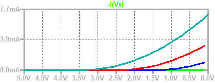
The first
task the student was assigned was to experimentally generate the following
plots for the MOSFETs.
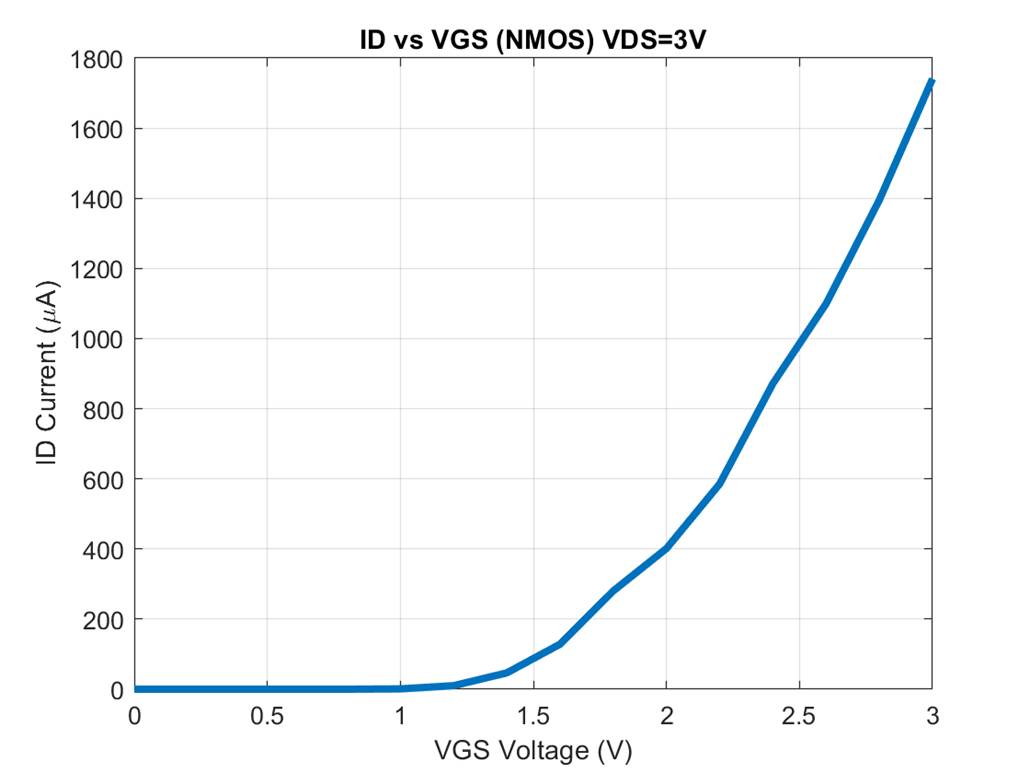
NMOS Device Plots:
1.
ID
v. VGS (0 < VGS < 3 V) with VDS = 3 V.
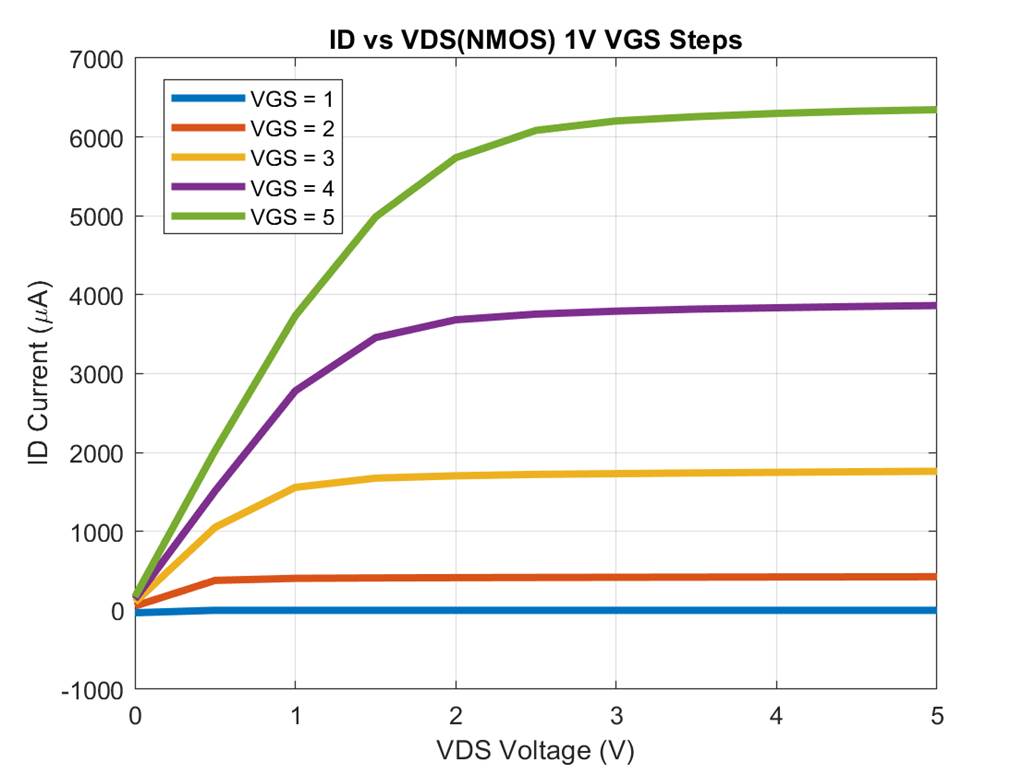
2.
ID
v. VDS (0 < VDS < 5 V) for VGS varying from 1 to 5 V in 1 V steps.
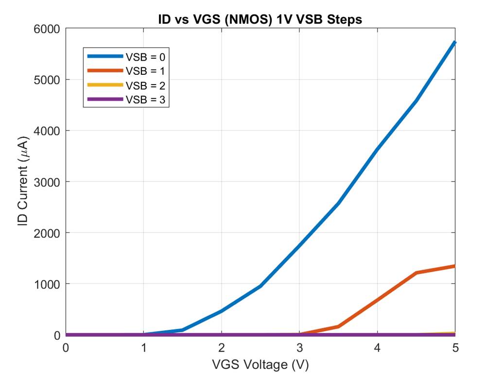
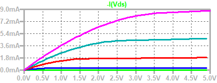
3.
ID
v. VGS (0 < VGS < 5 V) with VDS = 5 V for VSB varying from 0 to 3 V in 1
V steps.
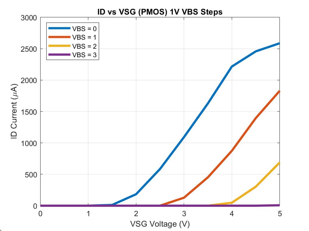
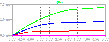
PMOS Device Plots:
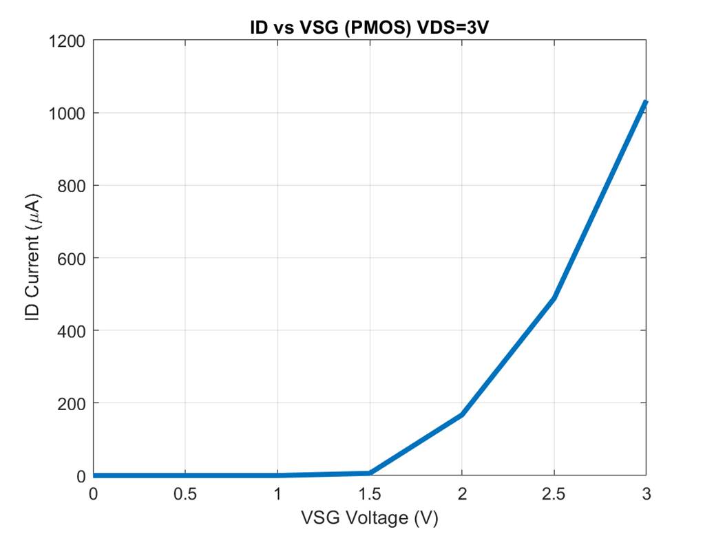
1.
ID
v. VSG (0 < VSG < 3 V) with VSD = 3 V.
2.
ID
v. VSD (0 < VSD < 5 V) for VSG varying from 1 to 5 V in 1 V steps.
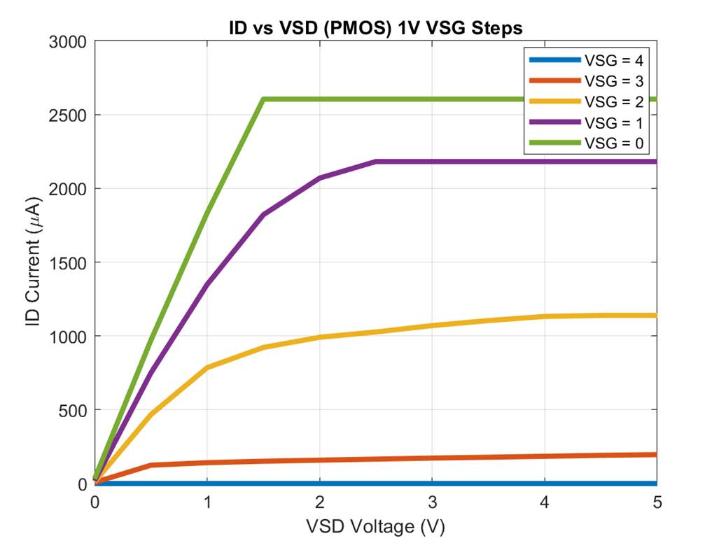
3.
ID
v. VSG (0 < VSG < 5 V) with VSD = 5 V for VBS varying from 0 to 3 V in 1
V steps.
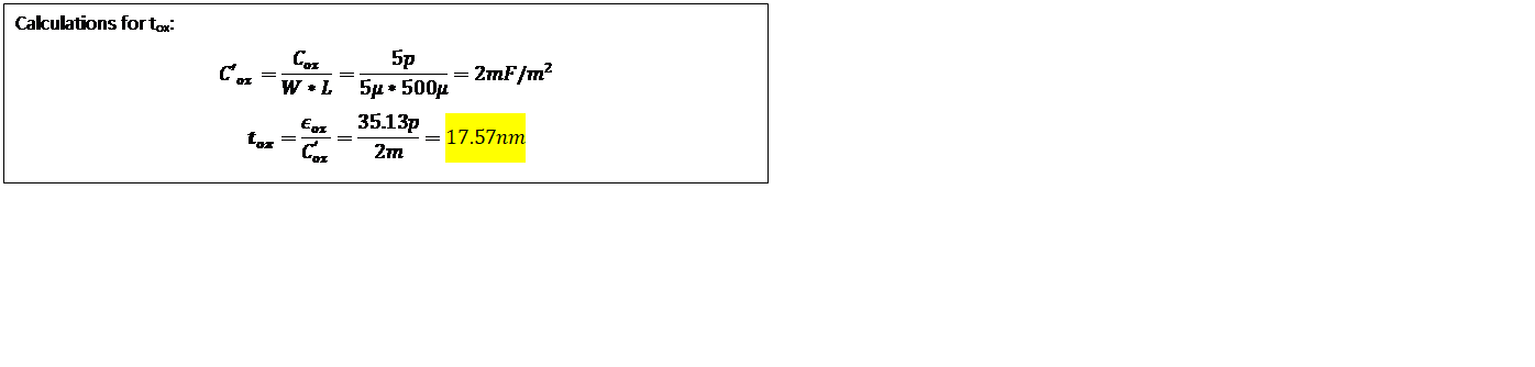
Following
the measurements and plots, the student was required to calculate oxide
thickness (tox) given the following.

tox for both
NMOS and PMOS was found using these equations:
The next lab procedure
had the student crate a level = 1 MOSFET model using the previously recorded
data. The level 1 model was required to have the following parameters in it:
VTO, GAMMA, KP, LAMBDA, and TOX.
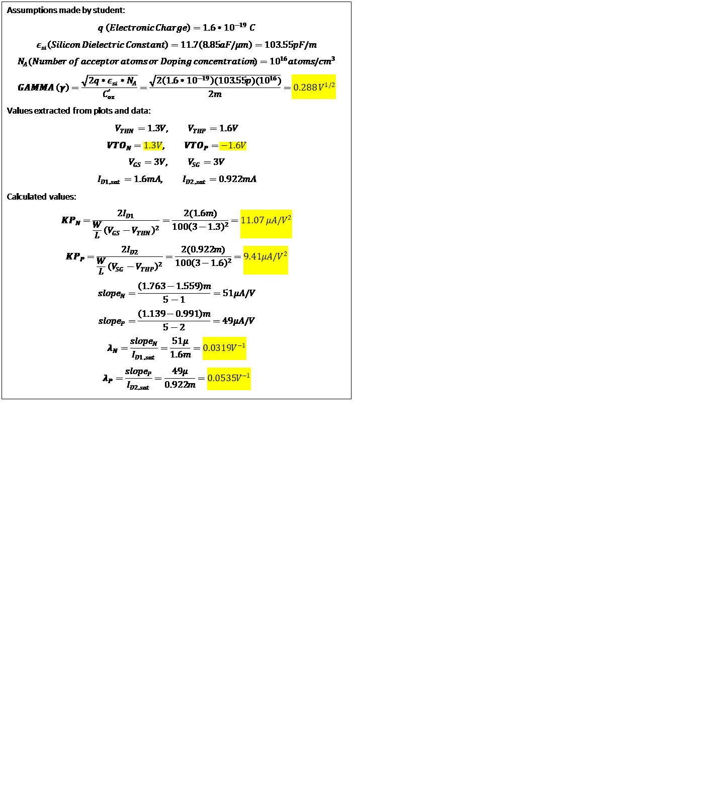
Using the calculated
values, an LTspice model text file was created that will be used for
simulations.
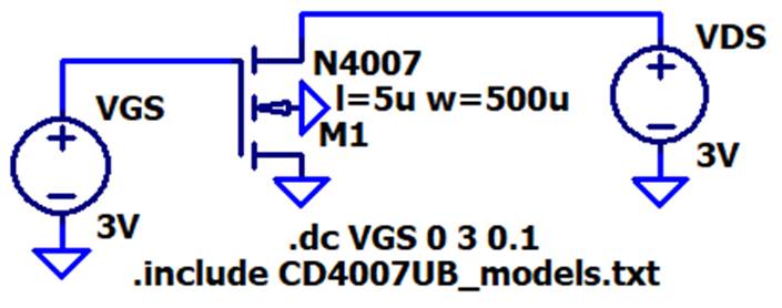
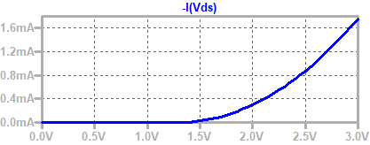
The next part of the lab
required the student to simulate the circuits on LTspice to recreate the plots
from the initial part of the lab.
NMOS Device Plots
(LTspice):
1.
ID
v. VGS (0 < VGS < 3 V) with VDS = 3 V.
2.
ID
v. VDS (0 < VDS < 5 V) for VGS varying from 1 to 5 V in 1 V steps.
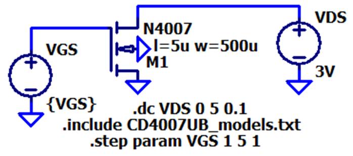
3.
ID
v. VGS (0 < VGS < 5 V) with VDS = 5 V for VSB varying from 0 to 3 V in 1
V steps.
PMOS Device Plots
(LTspice):
1.
ID
v. VSG (0 < VSG < 3 V) with VSD = 3 V.
2.
ID
v. VSD (0 < VSD < 5 V) for VSG varying from 1 to 5 V in 1 V steps.
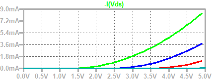
3.
ID
v. VSG (0 < VSG < 5 V) with VSD = 5 V for VBS varying from 0 to 3 V in 1
V steps.
The last part of the lab
required the student to experimentally measure the delay of an inverter using
the CD4007UB chip. In addition, the student is required to simulate the
inverter in LTspice using the model created.
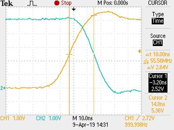
The student
experimentally measured that the delay of the inverter is 18ns.
Oscilloscope image measuring delay:
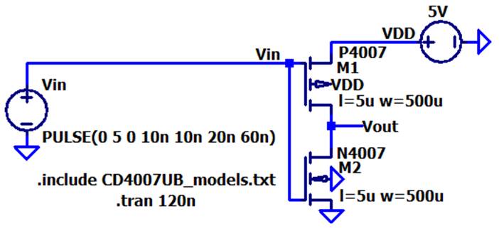
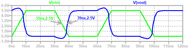
The student lastly created
the inverter circuit on LTspice and simulated it getting a delay of 9ns. The
simulation result was off by a factor of 2.
LTspice Schematic:
LTspice simulation:
This concludes lab 8.
Additional Links
→ Return to listing of
lab reports
→ Daniel’s CMOS
homepage
→
Dr. Baker’s CMOS homepage