 Lab 5 – EE
420L
Lab 5 – EE
420L
Authored by: Daniel Senda
Email: sendad1@unlv.nevada.edu
Spring 2019
Due: 03-13-2019
1) Introduction
The purpose of this lab is to
introduce the student to operational amplifier integrators. The student is
required to calculate characteristics associated with integrators as well as physically
test integrator circuits. In addition, the student is required to design an
integrator circuit to fit given requirements.
2) Pre-Lab Description
The
pre-lab required the student to do the following before proceeding with lab:
-
Watch the op-amp III
video and read op-amp_III.pdf
review.
-
Simulate the circuits given in the op-amp_III.zip
file and understand operation.
-
Read the entire lab write-up before going to class.
3) Description of Lab Procedures
This lab utilized the LM324
operational amplifier (op-amp). The datasheet can be found here.
The student was
asked to answer the following questions assuming VCC+ = +5V and VCC – = 0V.
- Calculate the
frequency response of the following circuit. Ensure you show your clear hand
calculations.
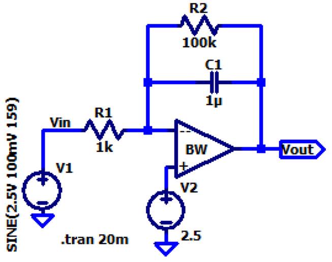
Schematic of integrator
circuit:
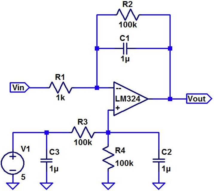
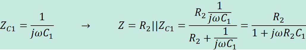
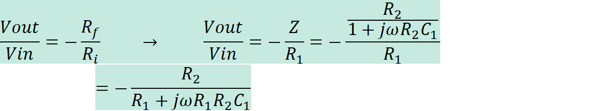
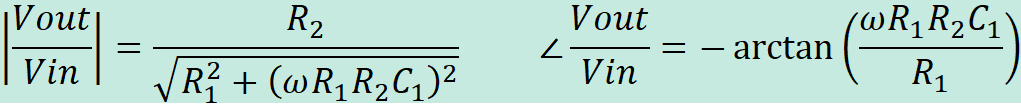
The following hand calculations show how to
calculate the frequency response of the
this circuit.
- What can you
neglect to simplify the calculation?
The student can neglect R2 in order to
simplify the calculation. This can be done because R2 is much bigger than R1,
so removing R2 from the equation will have a small effect on the results as can
be seen below.
![]()
![]()
- Does the circuit work if you remove
the 100k? Why or why not?
If the 100k resistor is removed from the circuit, it should
work but since the op-amp is not ideal there will be issues. The feedback loop
is no longer present affecting the offset, so the output signal may rail if the
input amplitude is too large.
- Does the 100k have much of an
effect on the frequency response?
The 100k resistor does not have much of an effect on the
frequency response of the circuit. The reason for this is because the value of
R2 is big compared to R1, so it’s almost as it was an open through R2 (infinite
resistance, which implies no resistor).
- Verify your calculations with
experimental results.
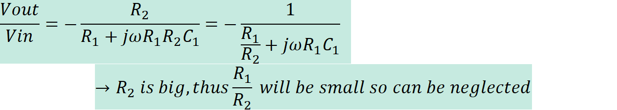
Waveform of circuit with R2 in
place:
As can be seen, there is a DC offset of about -1.64V on the
output signal.
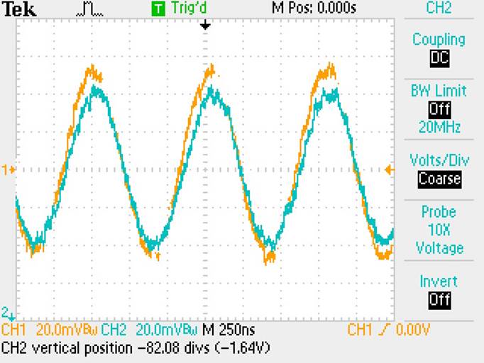
Waveform of circuit without R2:
If R2 is removed from the circuit, the DC offset is removed
from the output signal as demonstrated by the oscilloscope.
This results show how the DC offset changes depending
if R2 is present or removed.
- Show, at the unity-gain frequency
of the integrator, that the input and the output have the same peak values.
The following is the calculations for unity frequency.
![]()
![]()
Unity-gain frequency circuit
schematic:
Unity gain frequency waveform
results:
As can be seen from the waveform, the amplitudes of Vin and
Vout are the same.
- Is the phase shift between the
input and the output what you expect? Why or why not?
The phase shift between the two signals is -90 degrees,
which is what was expected by the student. The reason it was expected is because
capacitors are known to cause a -90 degree phase shift
in a AC signal.
The
last part of the lab had the student design, simulate, and build a square-wave
to triangle-wave generation circuit. The following instructions were given.
- Assume the input/output frequency
is 10 kHz and the output ramp must swing from 1 to 4 V centered around 2.5 V.
- Show all calculations and discuss
the trade-offs (capacitor and resistor values, input peak, min, and average,
etc.)
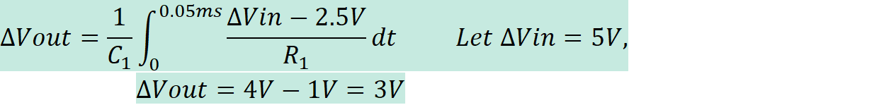
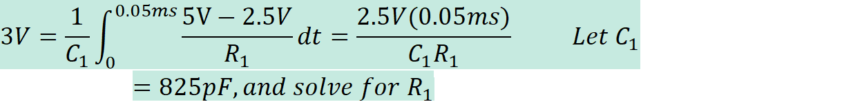
The
following is the calculations that were made to design the required circuit.
![]()
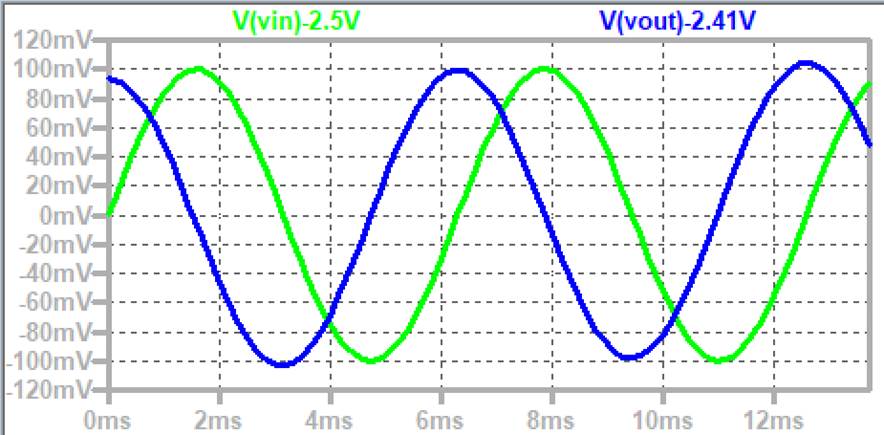
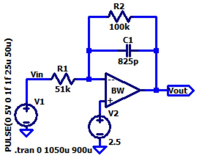
Designed circuit schematic:
Designed circuit simulation
waveform:
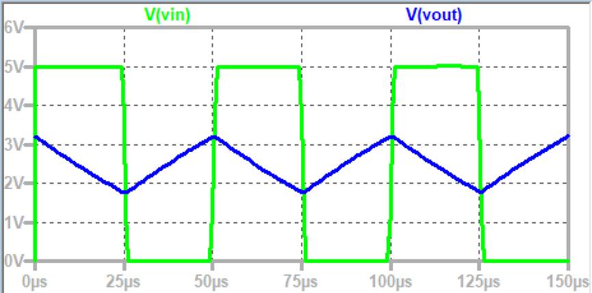
The waveform shows that the output is swinging in-between 1 to 4 volts. In order to get a swing of exactly 1 to 4 volts, the R1
value should be reduced to 25k ohms.
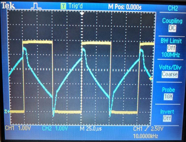
The
circuit was then created in the breadboard and the following waveform was generated.
As can be seen, the output is close to the design requirements. It does have
some unwanted noise, but is there because the built
circuit is not ideal.
Oscilloscope
waveform of built circuit:
Some of
the trade when designing this circuit is component values. If a smaller resistor
is what is available, then a bigger capacitor value will result from the
calculation. From experimental experience when building this circuit, it seems
that a smaller capacitor gives cleaner results. Thus, if you have a bigger capacitor
because of small resistor value, the output will have a bit more noise. Also,
the designer needs to keep in mind that the peak values of the triangle wave
needs to stay between 0 and 5 volts, or else the signal will rail.
This concludes
lab 5. (Lab was backed-up on an external drive)
Additional Links
→ Return to listing of
lab reports
→ Daniel’s CMOS
homepage
→ Dr. Baker’s CMOS homepage