 Lab 3 – EE 420L
Authored by: Daniel Senda
Email: sendad1@unlv.nevada.edu
Spring 2019
Due: 02-20-2019
1) Introduction
This lab is intended to help students learn how to read the datasheets
of integrated chips (ICs) as well as demonstrate how useful they can be when
creating/designing circuits. It also shows students how datasheets can
facilitate the testing and/or troubleshooting of circuits.
2) Pre-Lab Description
The pre-lab
required the student to do the following before proceeding with lab:
- Watch op-amp video and read review.
- Simulate the circuits given in the op-amp zip file and understand
operation.
- Read the entire lab write-up before going to class.
3) Description of Lab
Procedures
This lab
utilized the LM324 operational amplifier (op-amp). The datasheet can be found here. The
student was required to read over the datasheet before proceeding.
The student
was asked to answer the following questions assuming VCC+ = +5V and
VCC – = 0V.
- Knowing the non-inverting input, Vp, is at the
same potential as the inverting input, Vm, (called
the common-mode voltage, VCM) what are the maximum and minimum allowable
common-mode voltages?
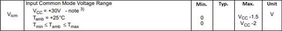
Looking at the datasheet, the minimum
allowable common-mode voltage (VCM) is 0V. The Maximum allowable VCM is: ![]()
- What is a good estimate for the op-amp's open-loop gain?
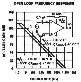
This graph is from the datasheet and it shows the open loop gain at
different frequencies. For example, at 100Hz the voltage gain is 80db.
- What is a good estimate for the offset voltage?
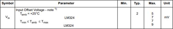
According to the datasheet, the typical offset voltage at ambient
temperature is 2mV.
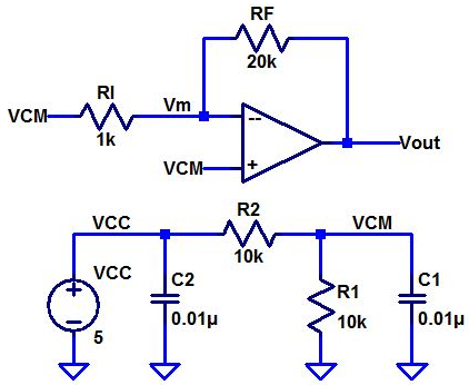
The next
part of the lab had the student build the following circuit on a breadboard.
(Note – The student used 5.1k ohms for RI and RF.)
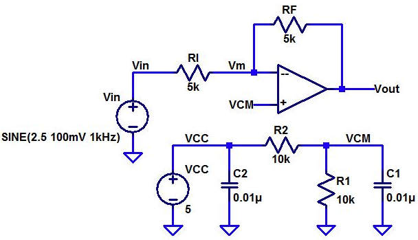
The
following questions were required to be answered with respect to this circuit.
- What is the common-mode voltage, VCM? Does VCM change? Why or why not?
The common-mode voltage (VCM) is the voltage that the sine wave revolves
around. VCM can change only if the resistor values of the voltage divider are
changed. Other that, VCM will remain constant.
- What is the ideal closed-loop gain?
The ideal closed-loop gain can be solved for from the following formulas:
Inverting Topology
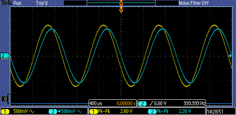
![]()
Vin in yellow and Vout
in blue:
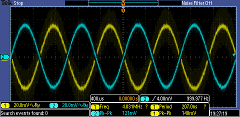
- What is the output swing and what is it centered around?
The output swing is the range that the output signal is restricted to.
For example in this circuit, the output swing ranged from 0V to 5V. The output
swing is centered around the VCM which is equal to 2.5V. (In other words, the
output swing is 2.5V above VCM and 2.5V below VCM.
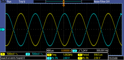
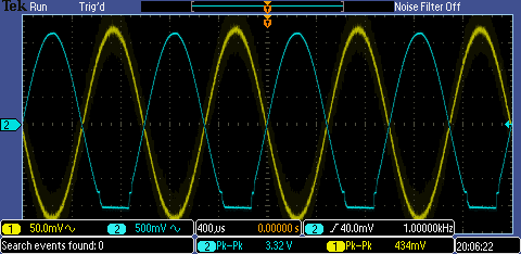
- What is the maximum allowable input signal amplitude? Why?
The maximum allowable input signal amplitude in this setup is 2.5V. The
is because the VCM is 2.5V and the gain is -1. The highest displacement voltage
is VCM + Vinmax = 2.5V + 2.5V = 5V. Since
VCC+ is 5V, the displacement voltage cannot go above 5V, thus the highest input
signal amplitude is 2.5V.
The output is still fine with a Vin
amplitude of 2.5V:
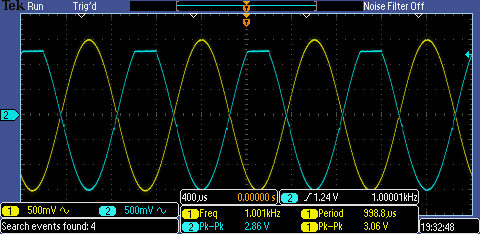
In this case, the amplitude of Vin is
greater than 2.5, which causes the output signal to clip the max displacement
voltage of 5 volts:
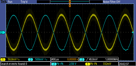
- What is the maximum allowable input signal if the magnitude of the gain
is increased to 10? Why?
If the gain of the op-amp is increased to 10, the maximum allowable input
signal is cut down by ten times. Again, this is because the peak voltage of Vin
should not pass the max displacement voltage of 5V. If it does pass 5V, the
signal will get clipped. This means maximum allowable amplitude for the input
signal is 250mV.
The output begins to distort a
slightly with Vin amplitude of 2.5mV:
Vin is 350mV. This causes the output
signal to clip:
- What is the point of the 0.01 uF capacitors
from VCC and VCM to ground?
The capacitors that are going to ground are decoupling capacitors. The
capacitors are used to help clean up the input signal and help decrease any
noise to get better signal representations on the oscilloscope. The values of
the decoupling capacitors are not too critical, as long as they are big enough
to reduce the unwanted noise. Usually, it is small noise that is needed to be removed so small capacitor values tend to be
sufficient.
- What is the input offset current? What does this term describe?
According to the datasheet, the LM324 op-amp has an input bias current of
about 20nA.The student changed RI and RF to very large resistances in order to
be able to see the affect that the input offset current has on the output. The
value resistances that were used were 30MΩ
resistors. Since the there is very little current
flowing because of the large resistances, the affect the bias current has on
the input/output can be seen.
The amplitude of the output starts to decrease due to bias current:
The student
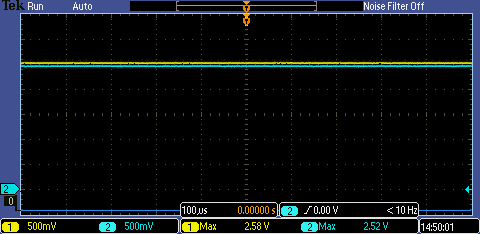
also had to measure the op-amp’s offset voltage. Following the schematic below,
the student creates the circuit on the bread board. Note – The student changed
RF to 100kΩ to increase the gain. The
increase of gain allowed to get better measurements of the offset voltage.
Circuit used to measure offset
voltage:
The op-amp
in this circuit has both V+ and V- inputs connect to the VCM voltage. Measuring
the difference of voltage between VCM and Vout will
therefore result in the value of offset voltage.
The student took
4 different LM324 chips and measured the offset voltages of them. The following
four images show the different offset of the chips. Further down below is a
table that organizes the data for easier reading.
Offset of 1st
LM324 chip:
Offset of 2nd
LM324 chip:

Offset of 3rd
LM324 chip:

Offset of 4th
LM324 chip:
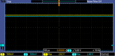
|
LM324 Chip |
Offset Voltage |
|
1st
Chip |
60mV |
|
2nd
Chip |
20mV |
|
3rd
Chip |
120mV |
|
4th
Chip |
160mV |
As can be
noticed, the offset voltages vary from chip to chip even though they are all
LM324s. One of the reasons for these differences is that chip manufacturing is
not an exact science. The die used for one “family” of LM324s can be slightly different
from the die of another family which causes the differences.
This concludes lab 3. (Lab was backed-up on an external
drive)
Additional Links
→ Return to listing of
lab reports
→ Daniel’s CMOS
homepage
→
Dr. Baker’s CMOS homepage