 Lab 1 – EE 420L
Authored by: Daniel Senda
Email: sendad1@unlv.nevada.edu
Spring 2019
Due: 01-30-2019
1) Introduction
-Lab 1 is intended to help students refresh their knowledge of
basic circuit fundamentals. The lab procedures go over basic RC circuits and
common calculations that are normally done for circuit
analysis.
2) Pre-Lab Description
-The pre-lab
consisted of the completion of the tasks listed below by the student:
- Request a CMOSedu account from Dr. Baker in order to publish lab
reports.
- Review the editing webpages
tutorial.
- Read the entire lab
requirements before going to class.
3) Description of Lab
Procedures
-The lab required
the student to simulate three circuits from the CMOS book using LTspice. Before
simulating, the student had to make hand calculations. These
hand calculations were then verified by the simulations. In addition,
the student had to verify the simulation results with experimental
measurements. This was accomplished by building the circuit on a breadboard and
using the appropriate lab equipment.
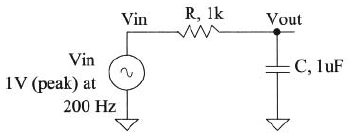
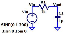
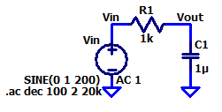
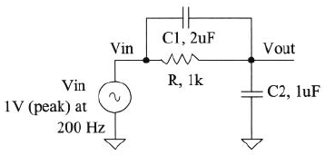
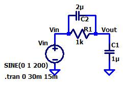
→ Circuit 1
Fig 1.21 from CMOS book: LTspice circuit schematic:
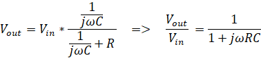
Hand Calculations:
-Below are calculations for circuit 1 including magnitude, phase, and time
delay of Vout.

![]()
![]()
LTspice simulation
results:
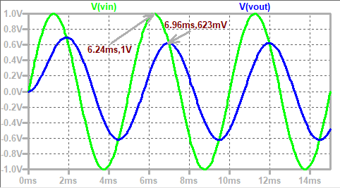
As can be noted, the magnitude and time delay (6.96 – 6.24 = 0.72s) of the
simulation waveform confirm the calculated values.
-The lab procedures also had the student do an AC analysis
for circuit 1.
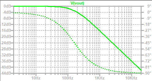
AC analysis circuit:
LTspice magnitude and
phase response waveform:
-Following
the LTspice simulations, circuit 1 was built and tested on a
breadboard.
Circuit 1 on
breadboard:

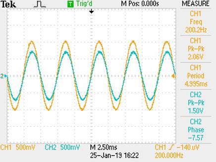
Oscilloscope waveform of circuit 1:
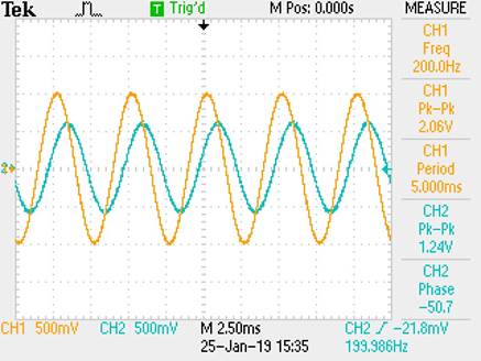
The oscilloscope results verified both the hand calculations and LTspice
simulation for the magnitude and phase of Vout.
Experimental data for AC analysis:
|
Frequency |
Vin |
Vout |
Phase |
|
2Hz |
1V |
1V |
0 |
|
20Hz |
1V |
0.98V |
-8 |
|
200Hz |
1V |
0.62V |
-51 |
|
2kHz |
1V |
0.1V |
-87 |
|
20kHz |
1V |
0.05V |
-89 |
Magnitude and phase response graphs
based on data:
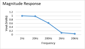
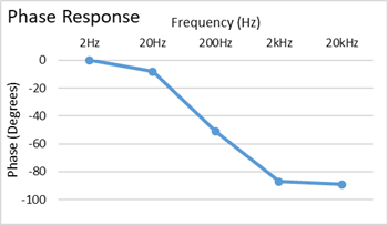
The frequency
response of circuit 1 according to the experimental data, is close enough to
the frequency response from the LTspice ac analysis.
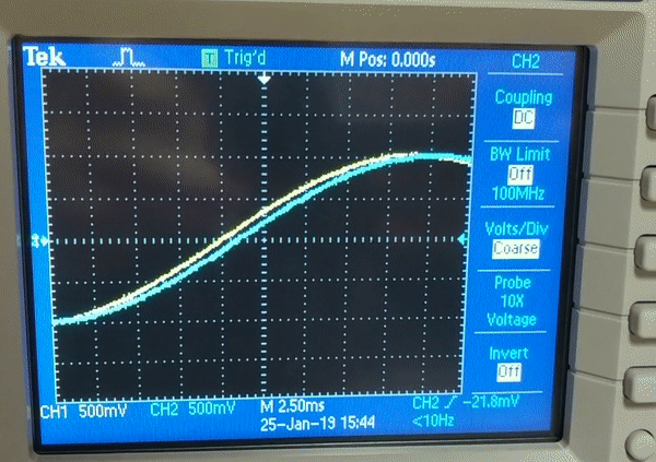
-As the
student was recording data, the student also swept the function generator in
order to see the magnitude of Vout
decrease as the frequency of Vin increased.
Down below is the results shown on the oscilloscope.
Loop of Vin and Vout as frequency increases:
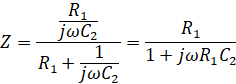
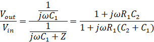
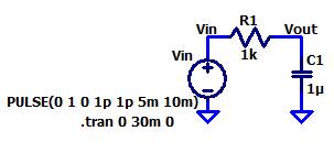
→ Circuit 2
Fig 1.22 from CMOS book: LTspice circuit schematic:
Hand Calculations:
-Below are calculations for circuit 1 including magnitude, phase, and time
delay of Vout.
![]()

![]()
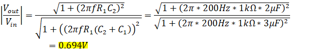
LTspice simulation results:
As can be noted, the magnitude and
time delay (6.34 – 6.25 = 0.09ms) of the simulation waveform confirm the
calculated values.
-Following
the LTspice simulations, circuit 2 was built and tested on a
breadboard.
Circuit 2 on
breadboard:
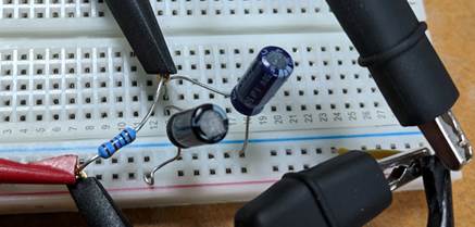
Oscilloscope waveform of circuit 2:
The oscilloscope results verify both the hand calculations and LTspice
simulation for the magnitude and phase of Vout.
→ Circuit 3
Fig 1.24 from CMOS book: LTspice circuit schematic:
Hand Calculations:
-Below are calculations for circuit 3 including RC time constant, charging
time, and frequency to complete fully charging and discharging.
![]()
![]()
![]()
![]()
LTspice simulation results:
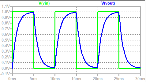
Based from the LTspice simulation waveform, it can be determined that the
calculated values are correct. It takes 5ms to fully discharge and 5ms to fully
discharge. This cycle can be done in a period of 10ms with a 50% duty cycle.
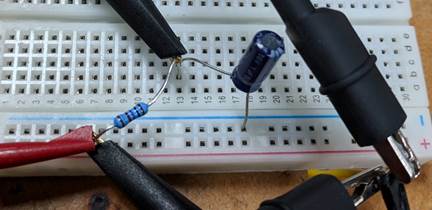
-Following the LTspice simulations, circuit 3 was built and tested on a breadboard.
Circuit 3 on breadboard:
Oscilloscope waveform of circuit 3:
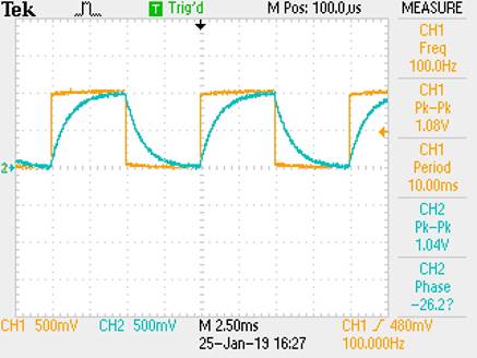
The oscilloscope results verify both the hand calculations and LTspice
simulation for charging and discharging times.
-This lab
and files were backed up.
-This
concludes lab 1.
Additional Links
→ Return to listing of
lab reports
→ Daniel’s CMOS
homepage
→
Dr. Baker’s CMOS homepage