 Final Project – EE 420L
Authored by: Daniel Senda
Email: sendad1@unlv.nevada.edu
Spring 2019
Due: 05-08-2019
1) Introduction
The final
project had the student use the skills and knowledge that they acquired throughout
the EE420 L to build a voltage amplifier. The student was given design
requirements that are required and need to be taken into consideration when
designing.
2) Description of Final
Project Procedures
The student was
given the task of designing a voltage amplifier with a gain of 10. The student
could use the ZVN3306A and/or the ZVP3306A MOSFETs and as many resistors and capacitors
as needed.
The
following table list the characteristic requirements of the design.
|
Characteristic Description |
Value/Range |
|
VDD Voltage |
Up to 9V |
|
Gain |
10 |
|
Input resistance |
Greater
than 50kΩ |
|
Minimum input frequency range |
100 Hz |
|
Amplifier load |
1kΩ |
|
Current draw under quiescent
condition |
Less than
or equal to 1mA |
In addition,
the student also had to try to get as fast of a design as possible while
driving the load and have as large of output swing as possible. AC coupling
input and output is acceptable.
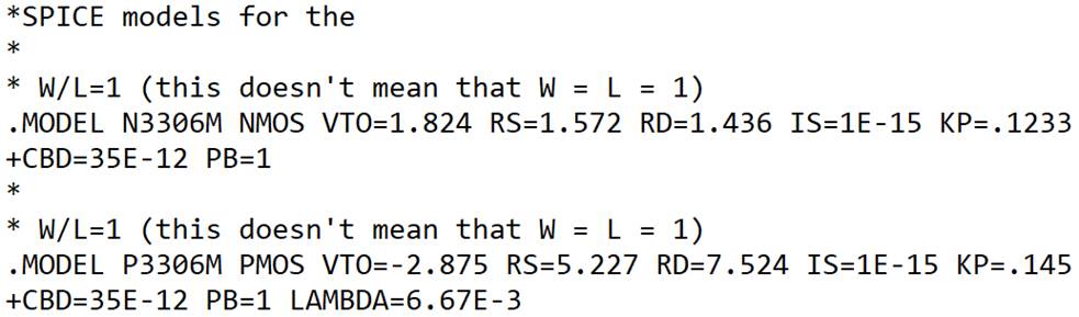
The student
went ahead and got values of variables that are needed from the spice models
text file shown below.
The first
step in the design process the student chose to follow was to get a better understanding
of the pros and cons from the different amplifier topologies. The following is
a list that has a few comparisons:
Common Source Topology:
· Has a large gain that is less than
zero, in other words negative value. (Av
< 0)
o
Degraded
by Rs
· Has a large input resistance (Rin>>)
o
Determined
by biasing circuit
· Has an output resistance that is approximately
RD (Rout = RD)
· ro decreases the gain and output
resistance (ro decreases Av and
Rout)
o
Impedance
seen looking into drain can be “boosted” by source degeneration
Common Gate Topology:
· Has a large gain that is greater than
zero, in other words positive value (Av < 0)
o
Degraded
by Rs
· Has a small input resistance (Rin<<)
o
Decreased
by Rs
· Has an output resistance that is approximately
RD (Rout = RD)
· ro decreases the gain and output
resistance (ro decreases Av and
Rout)
o
Impedance
seen looking into drain can be “boosted” by source degeneration
Source Follower Topology:
· Has a gain that is between 0 and 1 (0
< AV <= 1)
· Has a large input resistance (Rin>>)
o
Determined
by biasing circuitry
· Has a small output resistance (Rout <<)
o
Decreased
by RS
· ro decreases the gain and output
resistance (ro decreases Av and
Rout)
Using the
previous list of information, the student decided to make a two-stage amplifier.
The first stage of the amplifier consisted of a common source topology. The
second stage of the amplifier consisted of a source follower. The student chose
these topologies by taking the requirements into consideration as seen descried
below.
2-Stage Amplifier (Common Source to
Source Follower):
· The input of the 2-stage (common
source) has a large input resistance as needed.
· The output of the 2-stage (source
follower) can drive heavy loads like the 1k ohm requirement.
· The first stage will amplify the
signal to a gain higher than 10.
· The second stage can then reduce it
down to a gain of 10, and in addition can be able to drive a heavier load
without deceasing gain too much.
To bias the
first stage of the amplifier, the student had to determine an appropriate gate-source
voltage that would supply the desired bias current. The student decided to go
with 40uA for an ID. From there the student used LTspice to pinpoint a VGS
value that would result in that current.
NMOS biasing circuit:
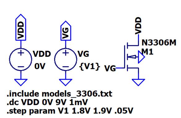
Resulting ID currents depending on VGS
value:
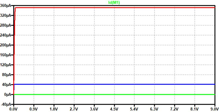
As can be
seen from the simulation, the student pinpointed that a VG=1.85V would result
in the desired 40uA. Now that these variables were found, the student went along
an calculated the bias circuit for the first stage (common follower).
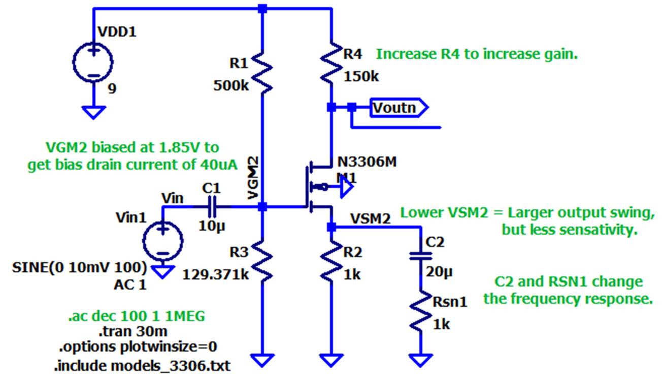
The following
is the source follower circuit (first stage) with correct biasing. A few of the
values were changed to compensate for other variables, for example power consumption.
Source Follower (1st Stage):
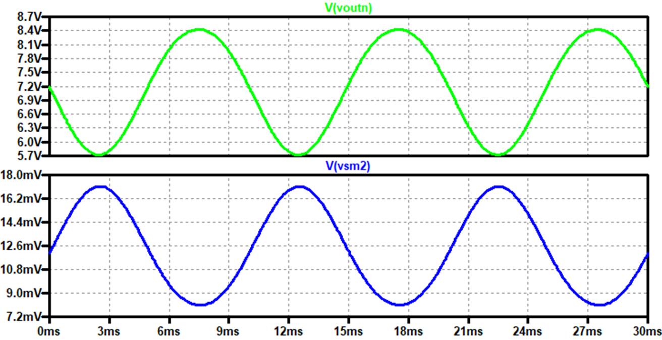
Simulation results:
Additional Links
→ Return to listing of
lab reports
→ Daniel’s CMOS
homepage
→
Dr. Baker’s CMOS homepage