Lab 9 – Design of a Beta-Multipler
EE 420L Analog IC Design
Lab Date: 4/10/19 Due: 4/24/19
Last Edited on
4/24/19 at 1:44pm using Word
NOTE: We will be using the CD4007UBE IC for
this Lab since the CD4007 CMOS IC was not available in the lab.
From Lab 8, we got to characterize the CD4007UBE CMOS
transistor array and have created the Level=1 MOSFET model in LTSpice. In this lab, we will be using this CMOS IC to
create a Beta-Multipler Reference Circuit.
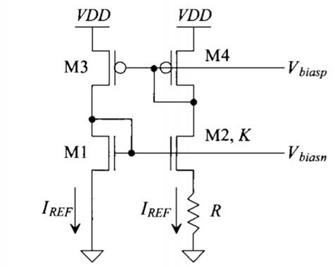
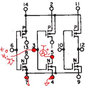
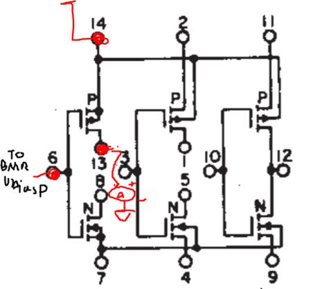
The Beta-Multipler Reference (BMR) circuit uses a PMOS current
mirror that sources current into an NMOS current mirror, and the source of one
of the NMOS transistors is connected to a resistor that is also connected to
GND.
Suppose we
have a BMR circuit with a K multiplier as shown:
So,
VGS1 = sqrt(2xI
/ [Kp x (W/L) ] ) + VTH,
VGS2 = sqrt(2xI
/ [Kp x K(W/L) ] ) + VTH,
VBiasN
= VGS1,
VGS1 – VGS2 = I x
R
Factoring out a square root and
eliminating VTH,
[ sqrt(2xI / [Kp x (W/L) ] ) ] x [ 1 – (1/K) ] = I x R
Squaring both sides:
(2xI / [Kp
x (W/L) ] ) x [ 1 – (1/K) ]2 = I2
x R2
Now dividing by I on both sides and
solving for I:
I
= (2 / [Kp x (W/L) x R2] ) x [ 1 – (1/K) ]2
If K=1, the IREF
from the PMOS current mirror will make the NMOS transistors have the same VGS,
thus, VBiasN = VGS = VG
– 0V and meaning that the voltage at source of M2 is 0V (NO CURRENT).
--------------------------------------------------------
Experiment 0: Prelab Content
~Note: We will
also be solving for R so that the NMOS devices have a gm of 20uA
Prelab
Simulation:
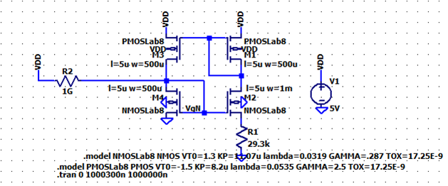
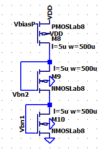
KpN = 11.07uA/V, W/L = 500μ/5μ,
K multiplier = 2, NMOS M2 W/L = 1m/5μ
Gm equation in
terms of ID:
Gm = sqrt(2 x ID x KpN
x (W/L) )
ID
= gm2 / [ 2
x KpN x (W/L) ]
ID
= 20μ2 / [ 2 x 11.07μ x (500/5) ]
ID = 180.6nA
BMR eqn in terms of ID and solving for R:
R = sqrt[ (2 / [Kp x (W/L)
x ID] ) x [ 1 – (1/K) ]2 ]
R = sqrt[ (2 / [11.07μ x (500/5) x 180.6n] ) x [ 1 – (1/2)
]2 ]
R = 29.3kΩ
A 1GΩ was
chosen as the start-up circuit so that theoretically (and assuming
that the voltage at the NMOS gate = 0V) the current that runs through
the resistor would be (5 – 0) / 1G = 5nA,
enough to drive the NMOS gate up, but not so much so that the start-up circuit
would cause the BMR to be unstable.
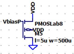
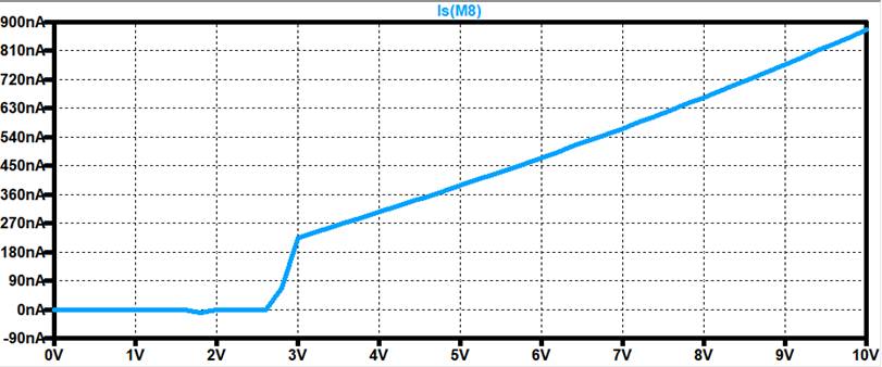
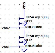
LTSpice:
Gm:
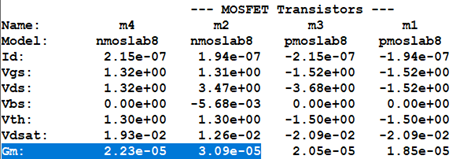
Current (.tran):
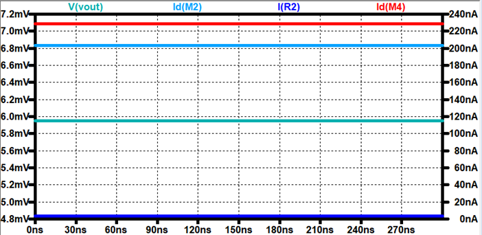
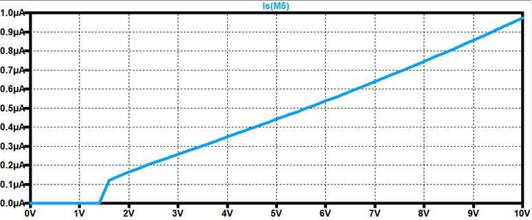
From the
Simulation, we are getting what we are getting around 200nA, which is in the
ballpark of what we want.
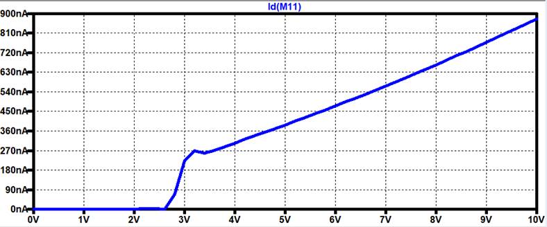
Voltage at
gates and Curernts (VDD Sweeping from 0V-10V):
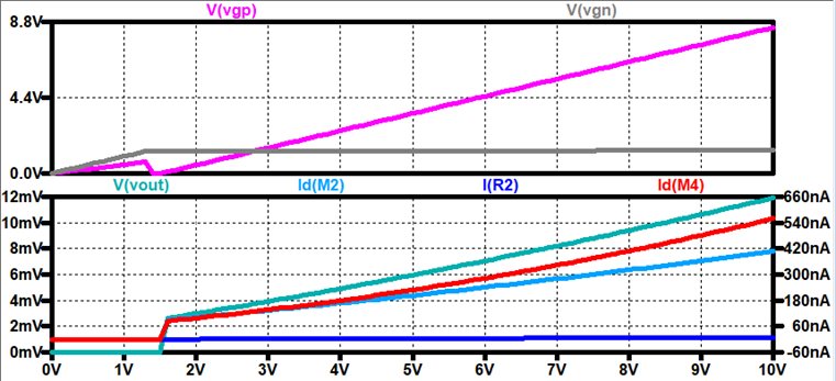
Experimental results:
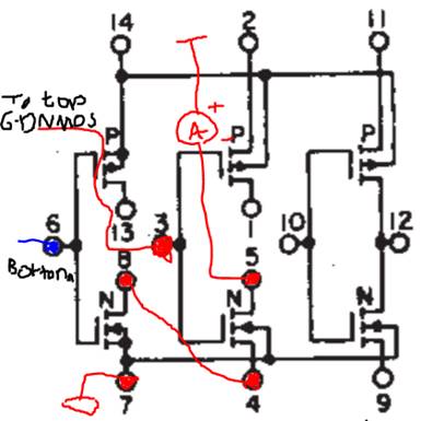
NOTE: For the NMOS
and PMOS BMR, we used 2 CMOS ICs, one for just the PMOS current mirror, and the
other for the NMOS current mirror. The K multiplier we chose was K=2, so we
used a 3rd IC to add another NMOS transistor.
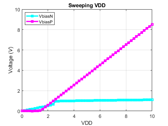
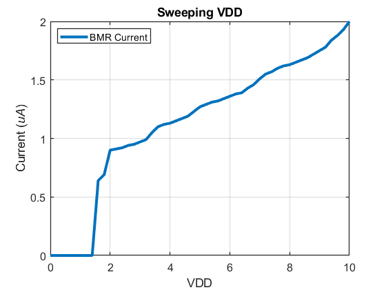
The current is
off by a factor of about 3, but keep in mind that we are using the NMOS models
used from the previous lab, and those were only approximations.
--------------------------------------------------------------------------------
SUPER NOTE (Toward
Future EE420L Students): When doing
this lab and using Analog Power Supplies that don’t have any smart-short
detector, PLEASE, try not connecting many CMOS ICs at one time. This lab will
require lots of preplanned transistor layouts, and it is easy to draw a lot of
current from the ICs. Start with the NMOS Current mirrors, and once done with
the cascaded PMOS, you can safely disassemble the NMOS current mirror and do
the PMOS current mirror.
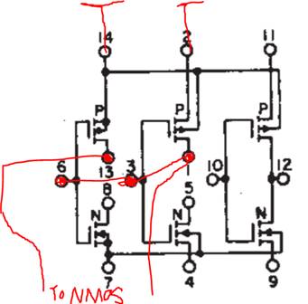
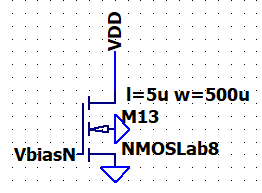
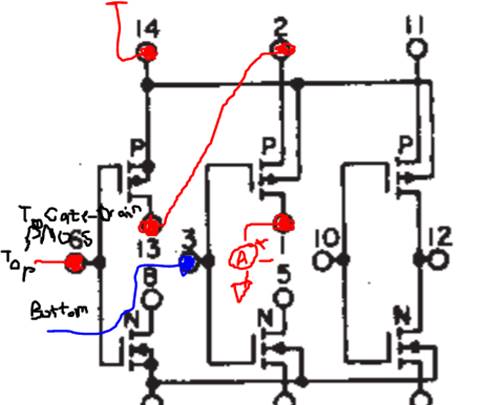
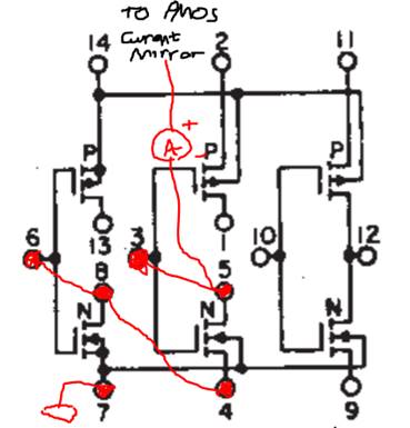
Experiment 1: NMOS Current
Mirrors
In this
Experiment, we will be building an NMOS current mirror. We will be using a new
IC to create the NMOS current mirror, and using the
NMOS gate voltage from the BMR to bias the NMOS current mirror. We will be also
measuring the current of the Current Mirror as we sweep VDD from 0V-10V.
LTSpice:
Experimental Results:
The current
running in the experiment is about 3 times larger than the current running in LTSpice.
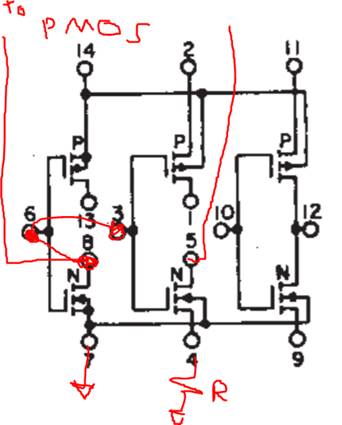
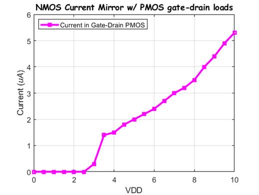
Now we will be
using this Current mirror to drive two (2) gate-drain connected PMOS devices on
a different IC. We will also be measuring the current in this load.
LTSpice:
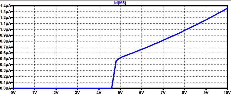
Experimental
Results:
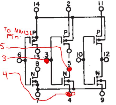
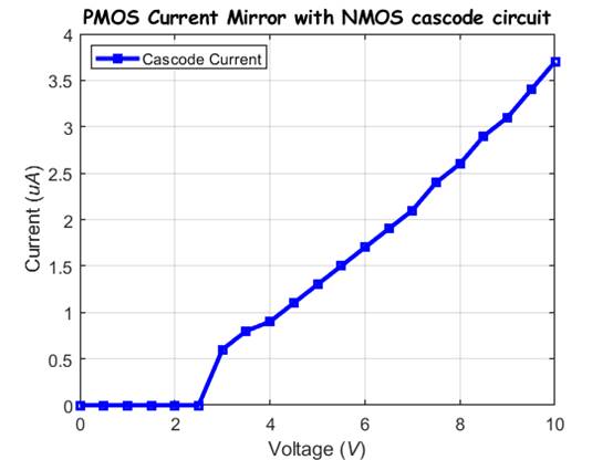
Now, we will
be building a Cascode PMOS Current Mirror using the
Gate voltages of the Gate-Drain PMOS device, and also
measuring the current in the cascode circuit.
LTSpice:
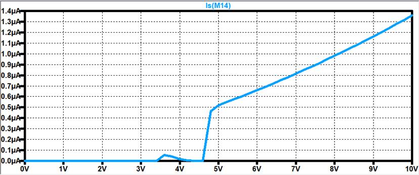
Experimental
Results:
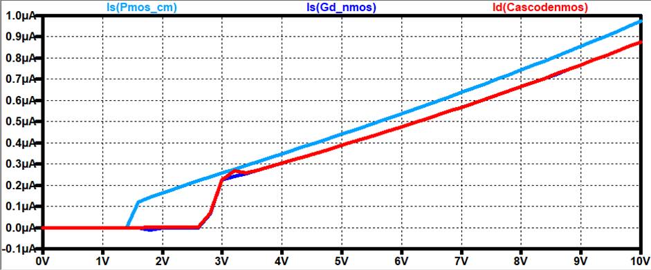
Now lets put all of the currents on one graph:
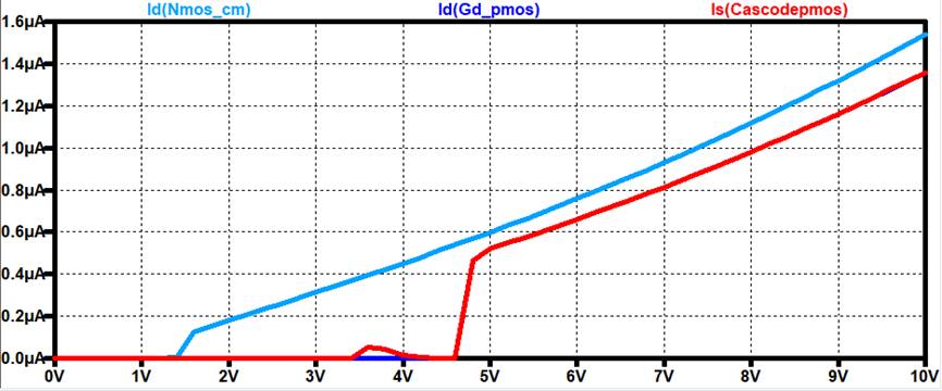
From this, we
can see that the NMOS current mirror current (Cyan) and the
current in the load that it is driving (Magenta) are nearly
the same. The current running through the NMOS cascode
circuit (Black) is also a bit low, but is close to
matching the PMOS current mirror. This could be due to the different threshold
voltages of the NMOS and PMOS transistors.
---------------------------------------------------------------------------
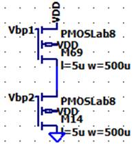
Experiment 2: PMOS Current
Mirrors
We will be
taking apart all the NMOS current mirrors and build the PMOS current mirror. We
will measure the current as VDD sweeps from 0V-10V.
LTSpice:
Experimental
Results:
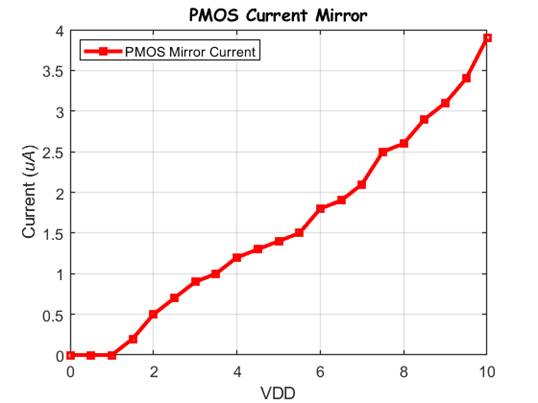
From this, we
can see that for the PMOS, we are off by a factor of 4 from LTSpice
simulations.
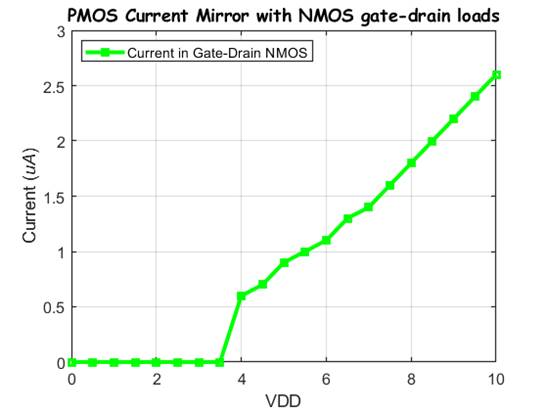
We will now
drive two (2) Gate-drain connected NMOS devices on a new IC.
LTSpice:
Experimental
Results:
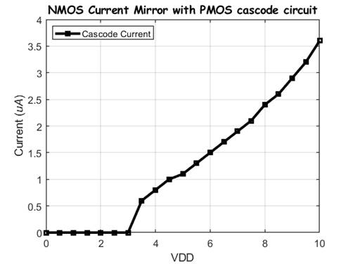
Now we will be
making a Cascode NMOS Current Mirror and biasing the cascode circuit with the voltage of the Gate-Drain
connected NMOS devices. We will be measuring the current of the Cascode NMOS current mirror as VDD sweeps from 0V-10V.
LTSpice:
Experimental
Results:
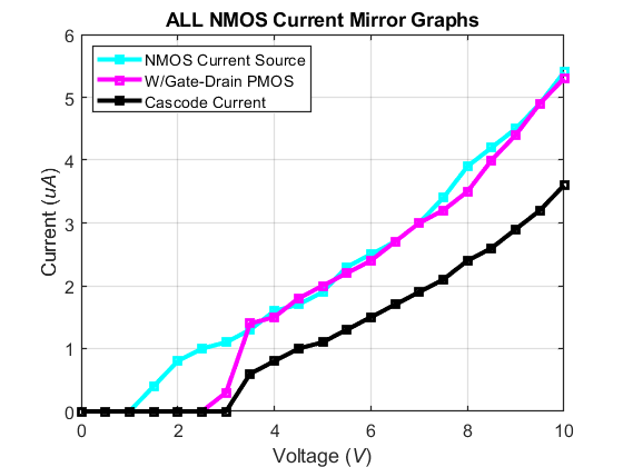
Placing all of the currents in one graph:
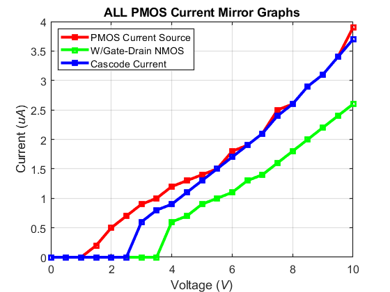
As we added a
load to the PMOS Current Mirror Source (Red), the current went down by
about half (Green). The NMOS cascaded current mirror (Blue), however,
matches the sourced Current mirror with the Gate-Drain Connected NMOS load.