Lab 8 – Characterization of the CMOS Transistor Array
EE 420L Analog IC Design
Lab Date: 4/03/19 Due: 4/10/19
By David Santiago – Email: santid4@unlv.nevada.edu
Last Edited on
4/09/19 at 10:45pm using Word
Super NOTE: We did not have the CD4007 chip available in the lab, so the TA
and Dr. Baker said that the CD4007UBE chip is okay. Values may be different.
Lab
description:
After using
NMOS transistors and PMOS transistors, we will finally be able to use a special
transistor called a Complementary Metal-Oxide Semiconductor, also known as:

CMOS
Transistor Arrays are basically NMOS transistors and PMOS transistors all in
one big tray of silicon.
In this lab, we
will be solving for the characteristics of the CMOS chip using experimental
results, and then using these characteristics and making our own Level 1 Model
transistors in LTSpice.
--------------------------------------------------------
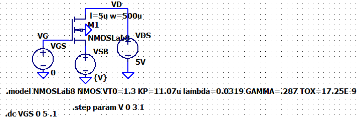
Part 1: The NMOS
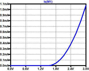
Experiment 1: ID vs VGS
In this
experiment, while VDS = 3V, we will be sweeping VGS and finding the current
values for ID.
Results:
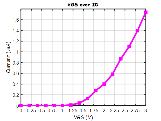
From looking
at this graph we can say that our Threshold Voltage can be around
VT0 = 1.3V
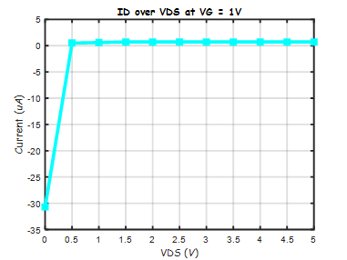
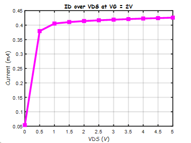
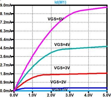
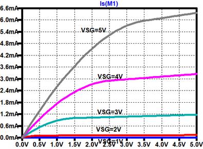
Experiment 2: ID vs VDS
In this
experiment, at different values of VGS, we will be sweeping VDS and recording
the values of ID.
At VGS = 1: NOTE this is in Microamps VGS
= 2:
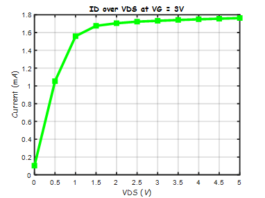
VGS = 3: VGS
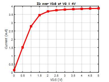
= 4:
VGS = 5:
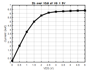
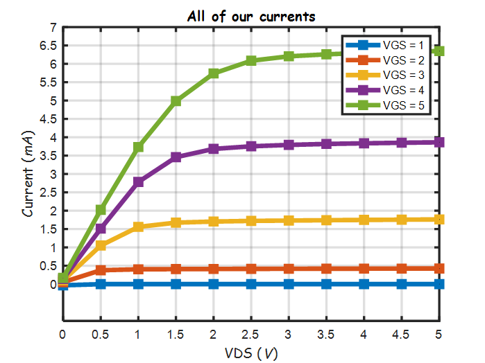
Now here is all of the VGS currents in one big graph:
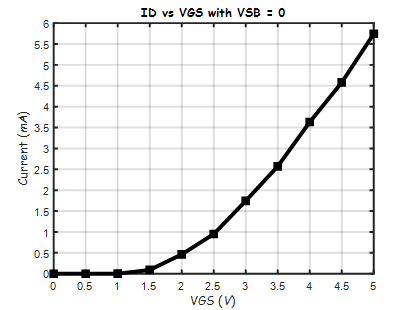
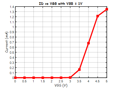
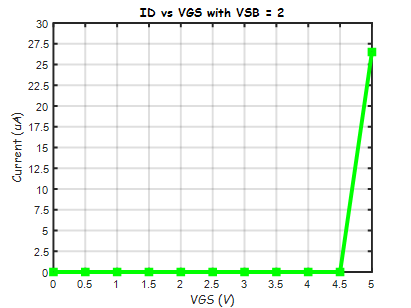
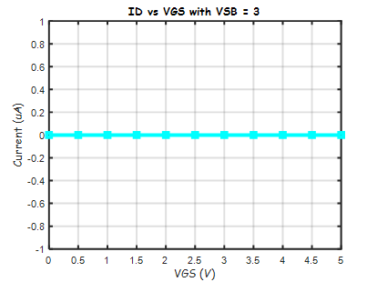
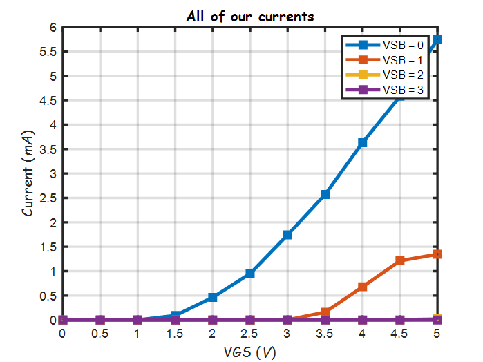
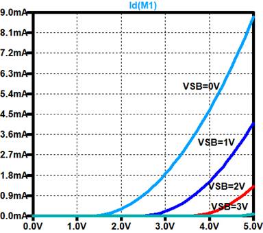
Experiment 3: ID vs VGS (With varying VSB)
In this
experiment, we will be changing VSB by grounding VB and applying a positive
voltage at VS.
At VSB = 0: VSB =
1:
VSB = 2: VSB
= 3:
Here is a
graph with all of the different VSB currents:
-----------------------------------------------------------------------------------
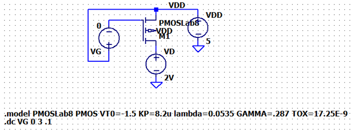
Part 2: The PMOS
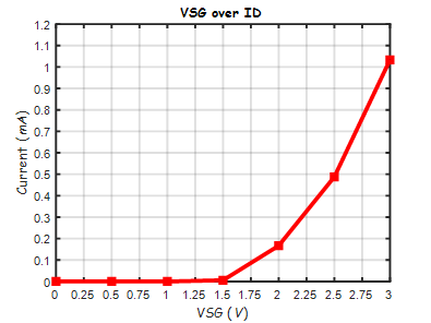
Experiment 1: ID vs VSG
We will do
everything we did for the NMOS but for the PMOS transistor.
Sweeping VSG from
0V to 3V with VSD = 5V – 2V = 3V
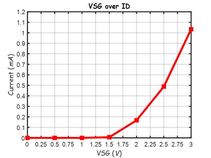
Threshold
Voltage = 1.5V, VT0 = -1.5V
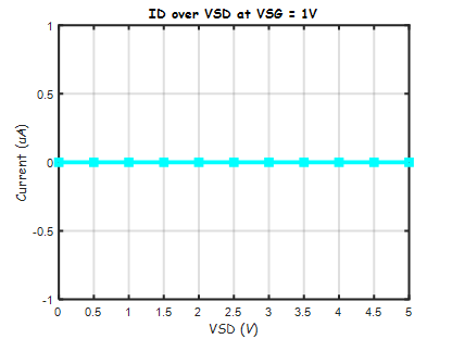
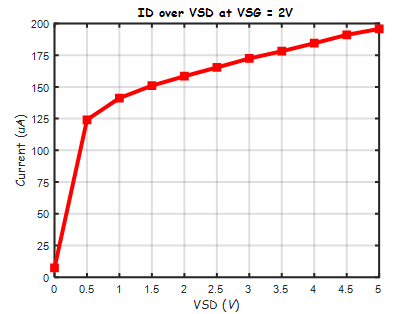
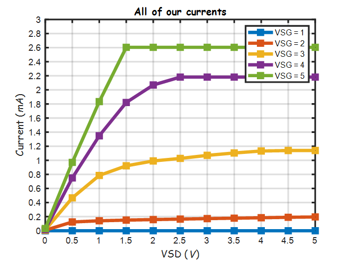
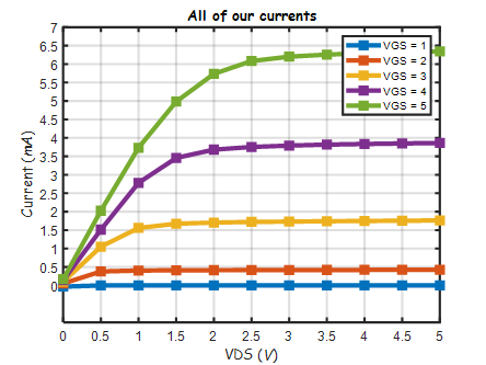
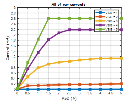
Experiment 2: ID vs VSD
Using
different VSG voltages, we will record the current ID over sweeping VSD.
BIG NOTE: As we keep
going to higher VSD voltages, our Battery source got to a point where it could
no longer let us have a higher VSG voltage. This could be due to the battery
source sensing that there is a “short” in the PMOS. Because of this we will
have INACCURATE measurements. For those higher VSD voltages at the higher
constant VSG, we used the same value as the highest max value of our VSG, so
the lines will look linear.
VSG = 1: VSG
= 2:
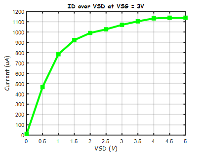
VSG = 3:
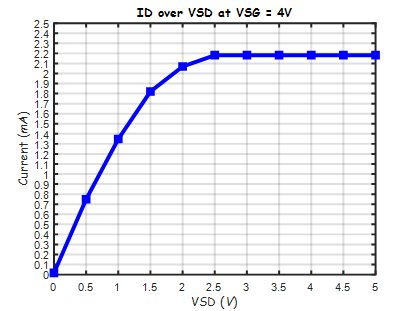
Highest VSD=4.5V VSG = 4:
Highest VSD=2.5V
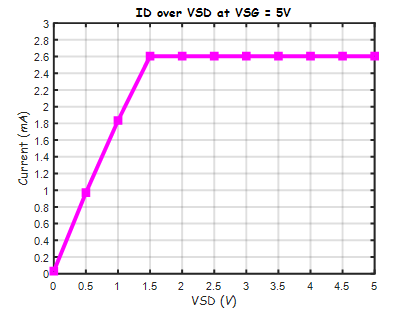
VSG = 5:
Highest VSD=2V
Here is all of our VGS currents:
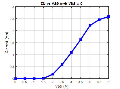
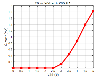
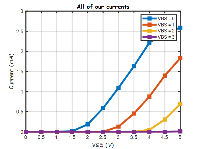
Experiment 3: ID vs VSG (With varying VBS)
In this experiment,
we will be connecting VB to VDD = 5V and changing VS.
VBS = 0V: VBS
= 1V:
VBS = 2V: VBS
= 3V:
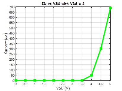
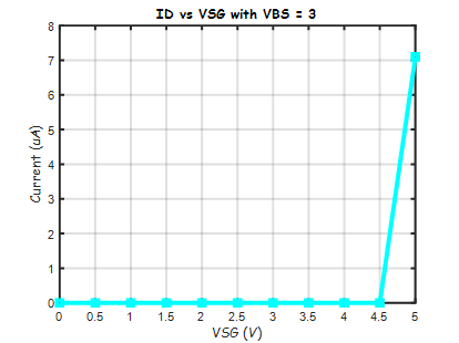
Here are all of the VBS curves in one graph!
Part 3: Figuring out the
Characteristics
Things that
need to be found: tox, VT0, Gamma, Kp, Lambda.
TOX
= εOX / C’OX εOX
=3.97* ε0 , ε0 =
8.85 x 10⁻¹² F/m
C’OX
= COX / (W*L), Given W = 500μm, L = 5μm, COX =
5pF
C’OX
= 2mF/m2
TOX
= εOX / C’OX = 3.97 x 8.85
x 10-12 / 2m
TOX = 17.57nm
VT0: For the NMOS, VTHN
= 1.3V VT0N = 1.3V
For the PMOS, VTHP = 1.6V, VT0P = -1.6V
Gamma: The
equation for Gamma given in the CMOS textbook:
Γ = sqrt(2 x q x εSI x
NA) / C’OX Given
that εSI = 11.7ε0, q
= 1.6 x 10⁻¹⁹ C,
NA
= 1016 atoms/cm3
Γ = sqrt(2 x (1.6x10-19) x (11.7x8.85x10-12)
x 1016/10-6) / 2x10⁻³
Γ = .287 V1/2
Lambda: From
Experiment: NMOS
Slope =
(1.763-1.559)mA/(5-1)V = 51μA/V ,
ID,SAT = 1.6mA, VGS = 3V
Given rO
= 1 / [ID,SAT x λ ], rO = 1/SLOPE,
ΛN
=SLOPE/ID,SAT = .0319 V-1
PMOS: Slope =
(1.139 - .991)m / 5-2 = 49.33μA/V
ID,SAT
= .922mA, VSG = 3V
ΛP
=SLOPE/ID,SAT = .0535 V-1
Kp:
Using the ID equation: ID
= Kp/2 (W/L) (VGS – VTH)2
Using
Experimental Values: Given W/L =
500μ/5μ = 100, ID = 6.83mA,
KpN
= 2ID / [ (W/L)(VGS – VTHN)2
] = 2(1.6m) / [ (100)(3 – 1.3)2
]
KpN = 11.07μA/V
KpP
= 2(.922m) / [ (100)(3-1.5)2]
KpN = 8.2μA/V
LTSpice Models:
NMOS:
NMOS VGS: Experimental:
From this,
even though we went by .2 increments, we got pretty close
to what our experiment says.
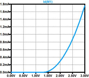
NMOS ID vs
VDS: Experimental:
From this, our
VGS=5V is a bit higher than our Experiment, and that could be due to how we can
calculate ID Saturation current and VVD,SAT.
But with 0.5V increments, this is in the ballpark and good for our simulations.
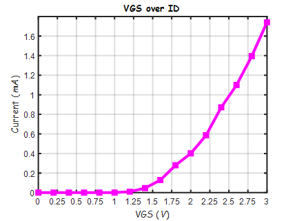
NMOS ID vs VGS
with changing VSB:

From this, our
VSB from the experiment would have been better if we used .1V increments due to
some of the points at the higher VSB. As we increase VSB, it will take much
more voltage VGS to get any current to come out of the NMOS.
PMOS:
PMOS VGS: Experiment:
From our LTSpice simulation (And from using only 0.5V increments),
we can say that we are also in the ballpark of making our simulations look like
our Experimental results.
PMOS ID vs
VSD: Experimental:
Because our
Battery Source would not let us sweep at a higher VSD at higher VSG voltages,
we had a harder time figuring out our lambda and our ID and VDS saturation
parameters. However, we did manage to get close, and are off by a magnitude of around 1.5.
PMOS ID vs VSG
with changing VBS:
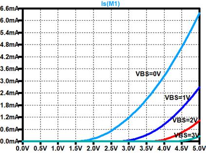
NOTE: Since
the gammas for the PMOS and NMOS are different and we are not given any way of
solving for gamma, we had to change the gamma parameter in LTSpice
to about 2.5. Due to the big error that our Battery source was giving us, this
is as accurate as we can get.
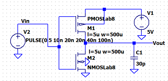
Part 3: The inverter:
Experiment 4:
In this
experiment, we will just be looking at how fast the Output reacts with the
input of the inverter and compare it with our LTSpice
models. We will have a small capacitance at the Probe tip, ideally 15pF, but
there will be some stray capacitance and we used 30pF to be safe.
Experimental:
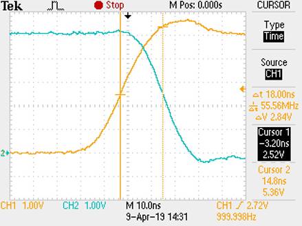
Delay =
18ns
Our Level 1 LTSpice Model:
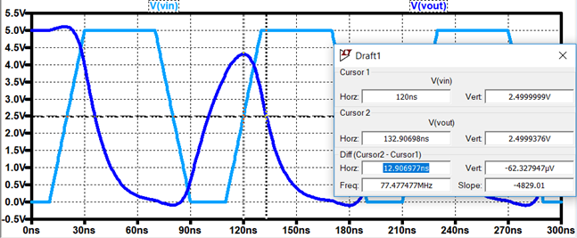
Delay =
13ns
From this, we
can say that we have made a great attempt at recreating our experimental CMOS
transistor array into LTSpice. We are off by a small
margin, but this is still good and we can say that
this is good for a Level 1 Model.