Lab 6 -
EE 420L
Authored
by: Roman Gabriele Ocampo
Email: ocampor5@unlv.nevada.edu
Date: Apri1 7, 2014
Single-Stage Transistor Amplifiers
Prelab:
- Review the ZVN3306A
and ZVP3306A
MOSFETs.
- Verify the behavior of the transistors in the
LTspice files provided on the lab page.
- Watch the video and review the notes located
provided on the lab page.
Lab
Description and Goals:
- Build the four amplifier circuits shown on the lab page:
the source follower, common source, common gate, and push-pull
amplifier.
- For each amplifier:
- Discuss the operation of the amplifier, including DC and
AC operation.
- Hand calculate the gain and the input/output resistance.
- Experimentally obtain values for the gain and the
input/output resistance.
Source Follower:
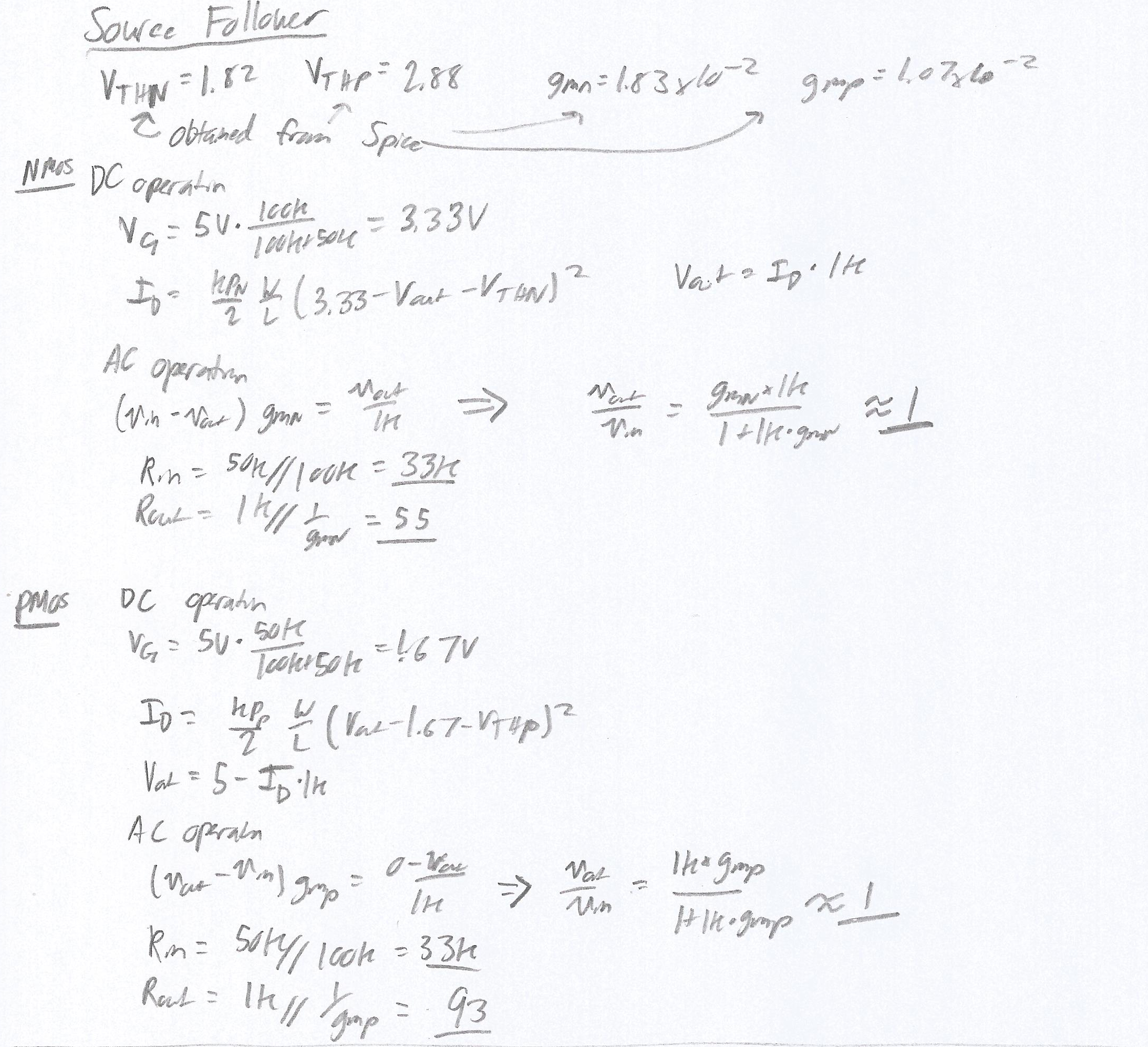
The following hand calculations illustrate the DC and AC operation of the Source Follower.

For NMOS:
Gain = 1, Rin = 33k, Rout = 55
For PMOS:
Gain = 1, Rin = 33k, Rout = 93
It can be seen from the simulation below that Voutn and Voutp are equal to Vin, meaning that the gain is 1V/V.


If
a resistor equal to the input resistance of the circuit is placed in
series with the input capacitors, then the output should be halved.
This is because of the voltage divider action occuring at the input.
Only half the input voltage is going into the amplifier, so only half
of the output will result.
From the hand calculations,
the input resistance for both NMOS and PMOS is 33k. The following
output waveforms are half that of the output during normal operation,
so the input resistance is indeed equal to 33k ohms.

If
a resistor equal to the output resistance is added in series with a big
capacitor (for biasing purposes) to the output node, the measured
output should be halved because the output impedence is doubled.
From
the hand calculations, the output resistance is 55ohms for NMOS and
93ohms for PMOS. The following output waveforms are approximately half
that of the output during normal operation, so the calculated output
resistances are accurate.

The experimental results are shown below.
NMOS
Gain:
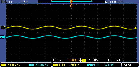
The amplitude of both input and output are just about equal, corresponding to a gain of 1V/V.
Rin:

To
measure Rin, add a 33k resistor before the capacitor. If the input
resistance of the amplifier equals 33k, then the voltage drop through
the 33k resistor should be half the input resistance. The waveform
above illustrates the voltage difference between the two sides of the
resistor. The voltage drop is half, so the input resistance of the
amplifier equals 33k.
Rout:

To
measure Rout, add a 56 ohm resistor in series with a big capacitor to
the output. Since the output resistance of the entire circuit has
doubled, you should expect to see half the output voltage of the
unmodified amplifier. The waveform above shows that the output is half
the input, while normal operation causes the output to be equal to the
input. Since the output voltage is halved, the output resistance is
equal to 56 ohms.
PMOS
Gain:
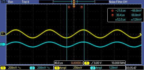
Vout/Vin = 128/200 = 0.64
The
experimental gain is smaller than the calculated gain. This is due to
the gm of the actual PMOS being different than the SPICE simulation.
This problem has come up frequently with all the PMOS circuits to
follow.
Rin:

To
measure Rin, add a 33k resistor before the capacitor. If the input
resistance of the amplifier equals 33k, then the voltage drop through
the 33k resistor should be half the input resistance. Thus, the output
voltage will be half of the output voltage of the unmodified amplifier.
72.0mV is about half of 128mV, so the input resistance equals 33k.
Rout:

To measure Rout, add a resistor equal to the calculated Rout in
series with a big capacitor
to the output.Since the output resistance of the entire circuit has
doubled, you should expect to see half the output voltage of the
unmodified amplifier. However, in the experimental circuit, adding the
calculated 93 ohms causes Vout to be zero. This is due to the Gmp of
the PMOS is different from what is given on the LTspice model. A
resistor of 390 ohms is used in the waveform above. The output voltage
is not exactly half of the unmodified amplifier, but it is a closer
estimate than 93 ohms.
Common Source:
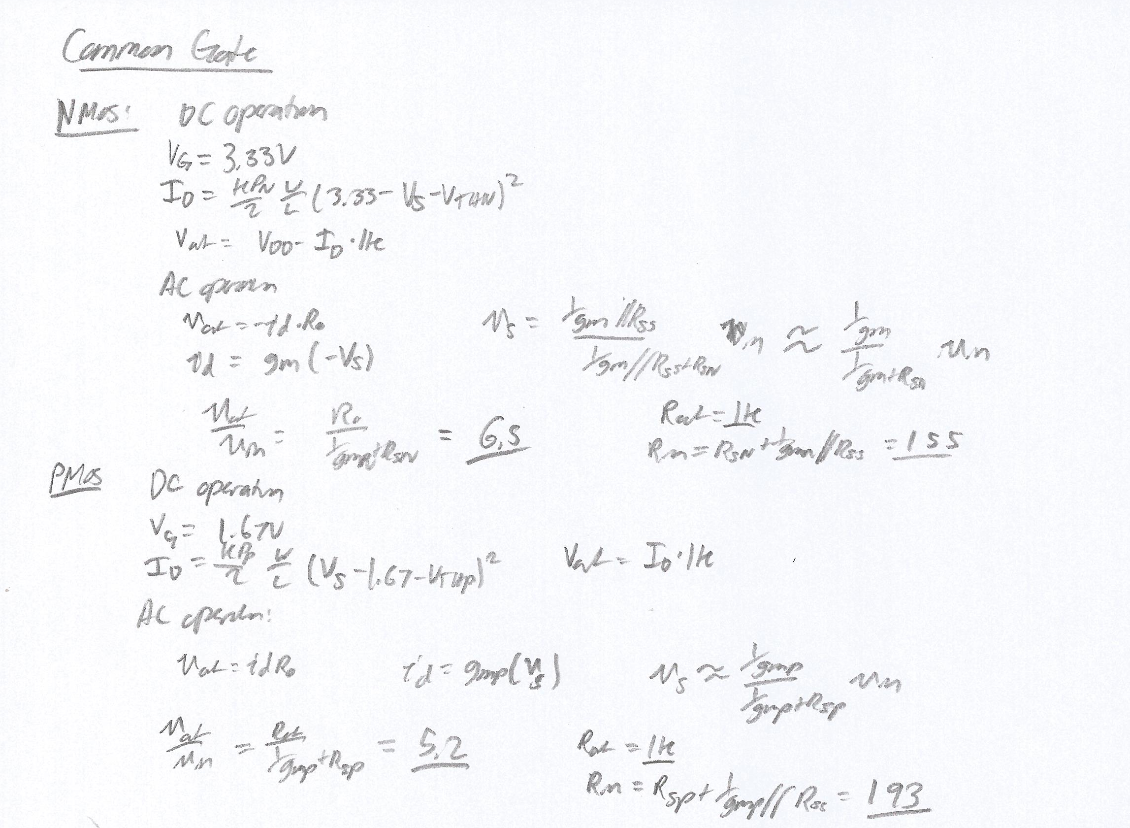
The following hand calculations illustrate the DC and AC operation of the Common Source amplifier:

For NMOS:
Gain = -6.5, Rin = 33k, Rout = 1k
For PMOS:
Gain = -5.2, Rin = 33k, Rout = 1k
From
the hand calculations, the source resistance (Rsn and Rsp) are found in
the denominators. Therefore, increasing the source resistance decreases
the gain, and vice-versa.
It can be seen from the
simulation below that the gain of the NMOS is 7 while the gain of
the PMOS is 5, both with 180 degree phase shifts.
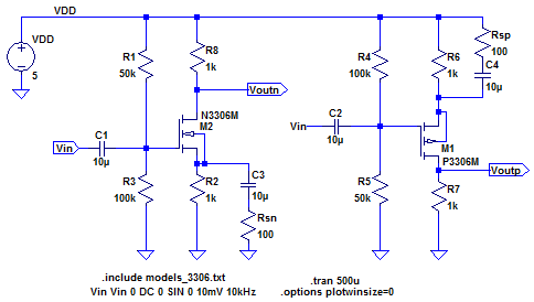

Using
the same logic from above, resistors equal to the input or output
resistance of the circuit added to the input or output (respectively)
causes the output to be halved.
With the addition of a
33k ohm resistor to the input, half the output results. Thus, the input
resistance is indeed equal to 33k ohms for both NMOS and PMOS.

With
the addition of 1k ohm resistors in series with a big capacitor to the
output node, half the output results as well. Thus, the output
resistance is equal to 1k ohms for both NMOS and PMOS.

The experimental results are shown below.
NMOS
Gain:
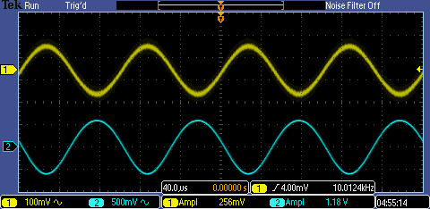
Vout/Vin = 1.18V/0.200V = 5.9V/V
Please
note that 200mV was used for the input amplitude (rather than the 256mV
shown on the scope) because this is the value manually entered into the
function generator.
Rin:

Including
a 33k resistor causes the amplitude of Vout to drop to 580mV, which is
approximately half of 1.18V, confirming the hand calculated Rin value.
Rout:

Including
a 1k resistor causes the amplitude of Vout to drop to 580mV, which is
approximately half of 1.18V, confirming the hand calculated Rout value.
PMOS
Gain:
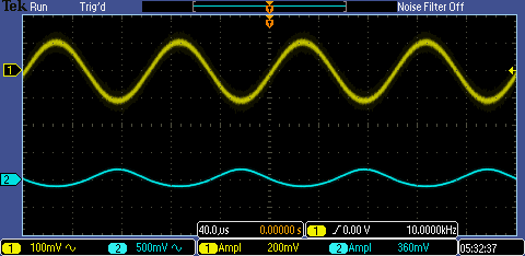
Vout/Vin = 360mV/200mV = 1.8V/V.
This
is much different than the hand calculated value. This is due to the
actual gm of the transistor being different from the spice model.
Rin:

Including
a 33k input resistance results in a 200mV output, which is
approximately half of 360mV, confirming the hand calculated Rin value.
Rout:
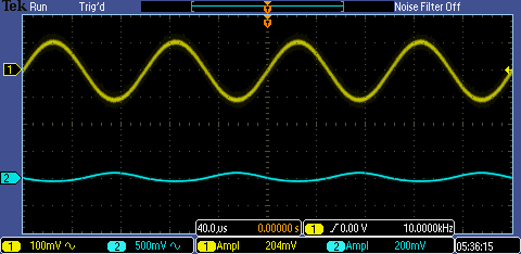
Including
a 1k output resistor causes the amplitude of Vout to drop to 200mV,
which is approximately half of 360mV, confirming the hand calculated
Rout value.
Common Gate:
The following hand calculations illustrate the DC and AC operation of the Common Gate amplifier:

For NMOS:
Gain = 6.5V, Rin = 155ohms, Rout = 1k
For PMOS:
Gain = 5.2, Rin = 192ohms, Rout = 1k
The
source resistance (Rsn and Rsp), are located in the denominators of the
gain calculations. Therefore, an increase in source resistance results
in a decrease in gain.
It can be seen from the simulation below that the gain of the NMOS is approximately 7 while the gain of the PMOS is 5.

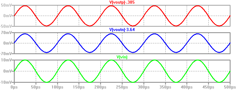
Using
the same logic from the past 2 circuits, adding resistors equal to the
input or output resistance of the circuit causes the output to be
halved.
With the addition of a 155 ohm resistor to the
NMOS input, and a 193 ohm resistor to the PMOS input, half the output
results. Thus, the input resistances are equal to 155ohms and 193 ohms
respectively.
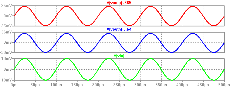
With
the addition of 1k ohm resistors in series with a big capacitor to the
output node, half the output results. thus, the output resistance is
equal to 1k ohms for both NMOS and PMOS.

The experimental results are shown below.
NMOS
Gain:
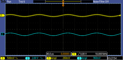
Vout/Vin = 960mV/200mV = 4.8
Rin:
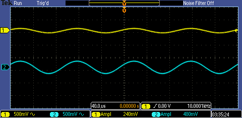
Including
a 155ohm resistor causes the output amplitude to drop to 480mV, which
is half of 960mV, confirming the hand calculated Rin value.
Rout:

Including
a 1k resistor causes the amplitude of Vout to drop to 400mV, which is
approximately half of 960mV, confirming the hand calculated Rout value.
PMOS
Gain:
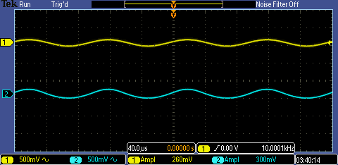
Vout/Vin = 300mV/200mV = 1.5V/V
Again,
this is much different than the hand calculated value. This is due to
the gm of the transistor being different from the spice model.
Rin:
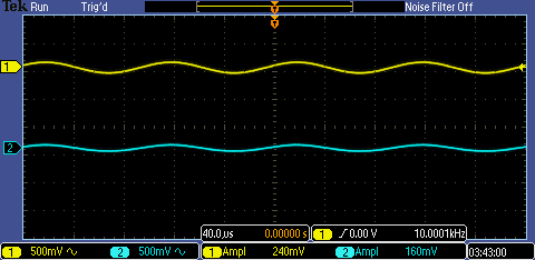
in
order to achieve this waveform, a 620ohm input resistance is used,
rather than the hand calculated 193. The transistor's difference in gm
is the cause of this discrepancy. The output voltage is 160mV, which is
approximately half of 300mV, confirming the 620ohm experimental input
resistance.
Rout:

Including
a 1k resistor to the output node causes the output to drop to 140mV,
which is approximately half of 300mV, confirming the hand calculated
Rout value.
Push-Pull
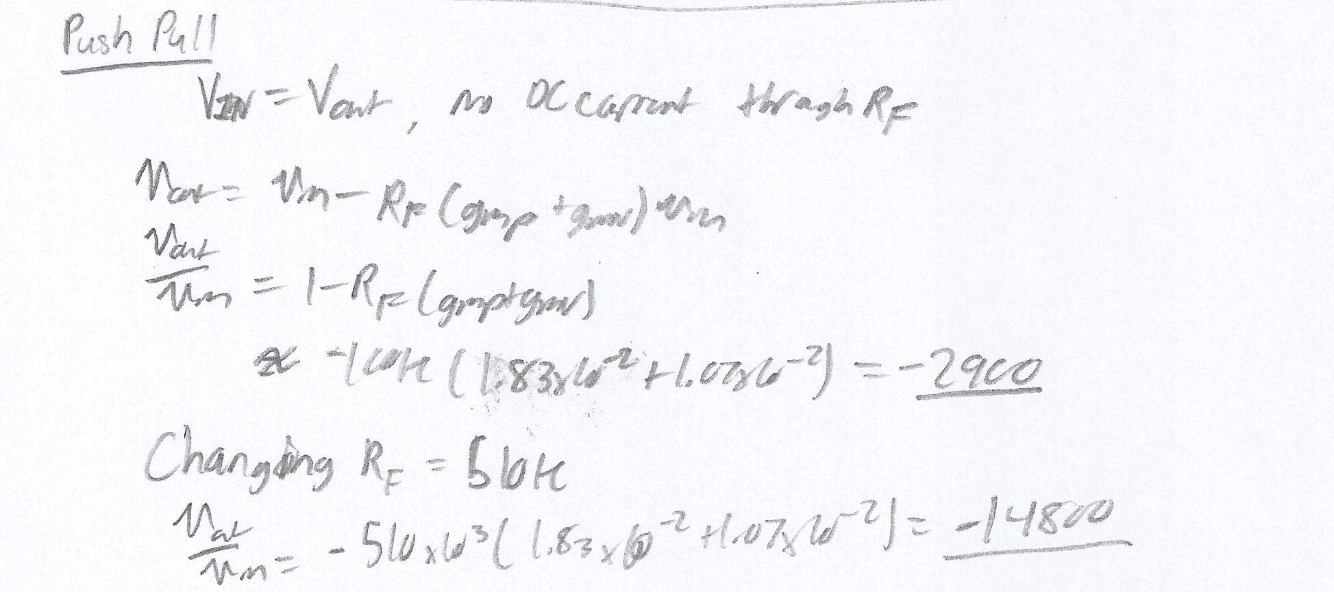
The operation for the Push-Pull amplifier is outlined in the hand calculations below.

Gain for RF=100k, -2900
Gain for RF=510k, -14,800
The schematic and simulation results are found below:
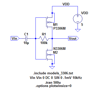

For a 100uV input, a 200mV output is generated (with a 180 degree phase shift). This corresponds to a gain of -2000.
The following waveform was achieved with an RF (R1 in this schematic) changed to 510k.
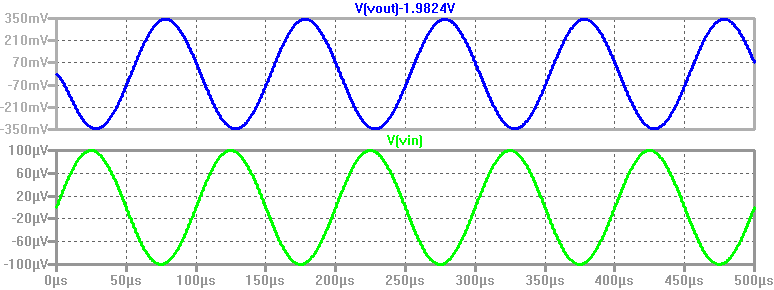
For a 100uV input, a 350mV output is generated (with a 180 degree phase shift). This corresponds to a gain of -3500.
It
is also worth noting that Vin=100uV is used in this experiment, rather
than the 100mV used in all the above circuits. This is because the gain
of the amplifier is so high that the transistor saturates at VDD and
ground, rather than fully amplifying the signal. This is shown in the
waveform below. the output voltage of the transformer cannot exceed
ground or VDD.

As
such, a voltage divider using a 10k resistor and a 10ohm resistor is
used to reduce the AC input voltage. This is shown below:

With this configuration, 0.1mV is the input voltage to the amplifier.
Using RF=100k

Vout/Vin = 240mV/0.2mV = 1200V/V
Return to the listing of my labs
Return
to the whole class reports
Return
to the EE420L site
Return to CMOSedu.com
