Silvaco EDA Tutorials from
CMOSedu.com
Tutorial
2 – Introduction to layout, pcells, and design rule
checking
In the first tutorial
we setup the schematic capture and simulation tools (Gateway,
SmartSpice,
and SmartView) for
ON’s
C5 process
and fabrication
through MOSIS using the
scalable CMOS (SCMOS) submicron
design rules where
the
scale
(Lambda) for the C5 process
using the SCMOS rules is 300 nm and the technology code is
SCN3ME_SUBM (info).
In
this tutorial we'll use Expert for drawing
layouts and Guardian DRC to design rule check the
layouts.
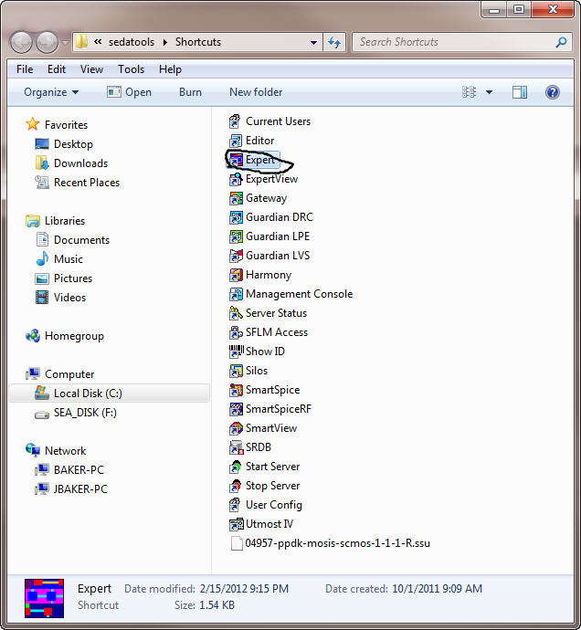
To
begin this tutorial start Expert by
double-clicking the LEFT mouse button on the icon seen below.
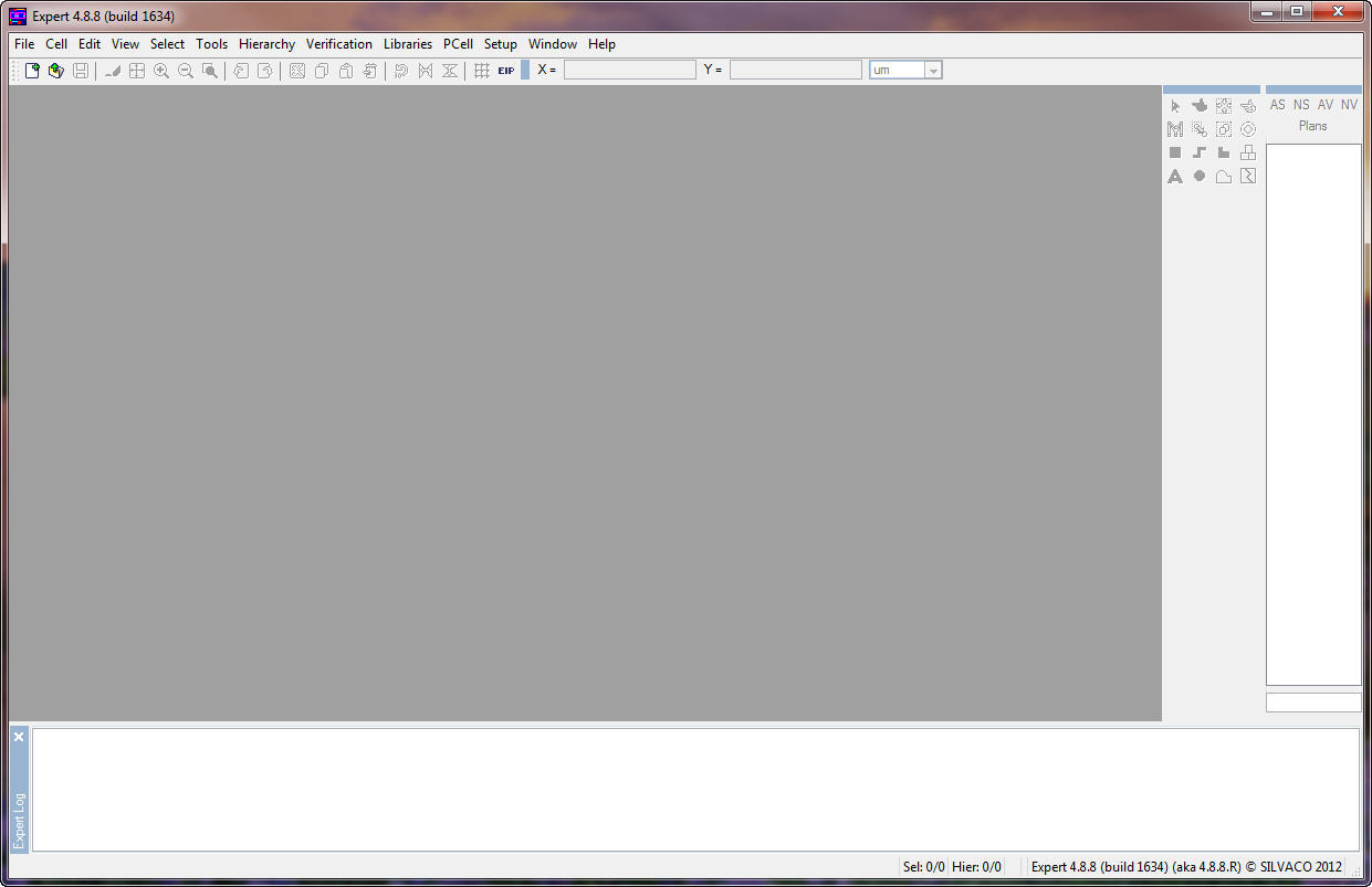
The following Expert
window will appear (where it's been re-sized to make it smaller for
this
tutorial).
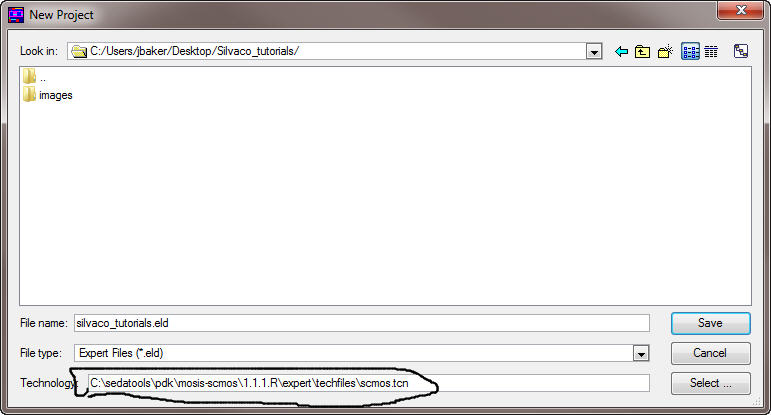
Next use File
-> New to make a new project, an *.eld (expert layout
design) file.
Call this project
"silvaco_tutorials.eld" and save it in the Silvaco_tutorials folder
on your desktop that your created in the first tutorial.
Before hitting the
Save button we need to attach a technology file to the project (to
setup the
layers, layer fill, etc.)
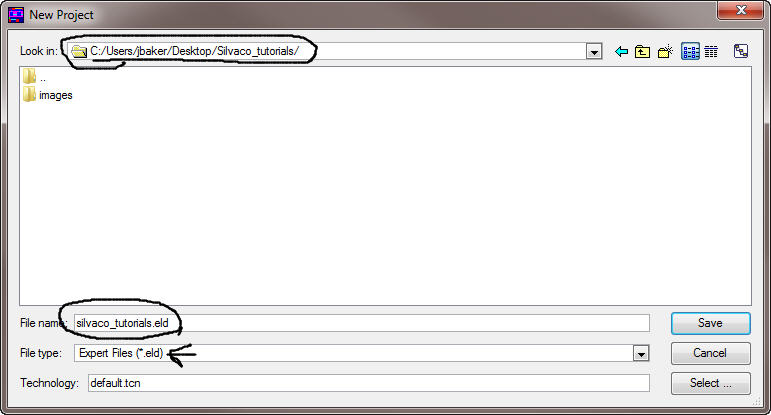
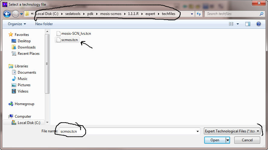
Press the Select
button and navigate to the MOSIS pdk (Process Design Kit) techfiles
directory
(below) and select the "scmos.tcn" expert technology
file (select by
hitting the Open button).
We are creating a
new project called "silvaco_tutorials.eld" that uses the MOSIS SCMOS
design rules.
Press the Save
button.
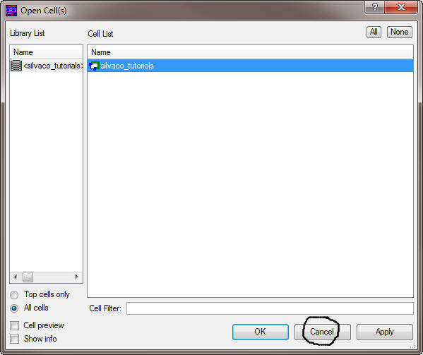
After pressing the
Save button we get the following window which shows the library name,
silvaco_tutorials,
and one cell
also called
silvaco_tutorials.
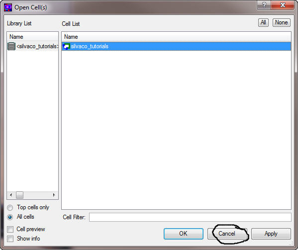
Select Cancel.
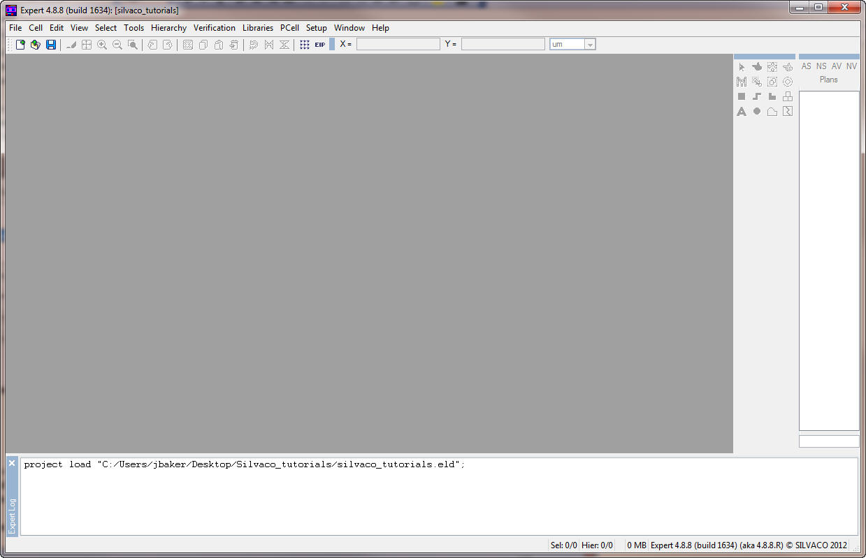
In the Expert
window that appears select File -> Save.
Use the menu and
go to Setup -> Technology -> General ->
Technology Setup ->
General and ensure "Use external technology file for *.eld
projects" is not selected as seen below.
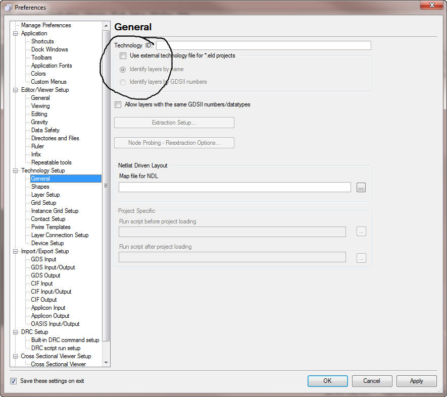
This is to ensure
that the technology file information, and any changes we make, is saved
in the silvaco_tutorials.eld
file.
Next time we open
the silvaco_tutorials.eld we don't need to specify a technology file.
Let's verify this
by closing Expert and re-starting it.
Use File
->
Open and notice now that the Technology field is grayed.
Select the Open
button.
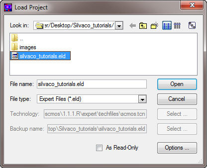
Again select
Cancel, as seen below, we don't want to open the silvaco_tutorials cell.
The following
window appears (again).
We next need to
setup the SCMOS pcells (parametric cells).
In a foundry
specific PDK the number of pcells is large. Here, in the generic MOSIS
SCMOS
pdk, the number is
smaller so we'll,
later in this tutorial, lay out additional building block cells.
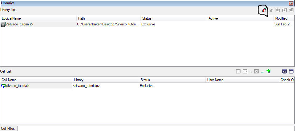
Use the menu Libraries
-> Setup then click on the Add
icon circled below.
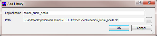
Navigate to the
scmos_subm_pcells.eld file seen below and then hit OK.
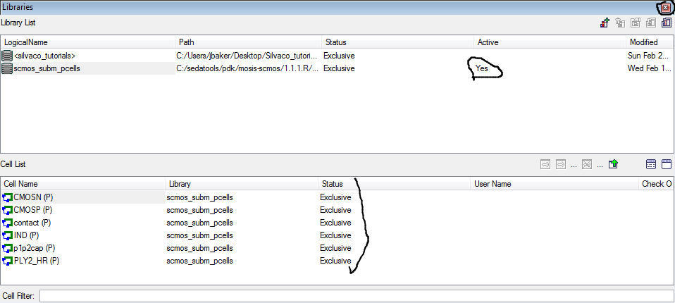
In the Library
List select "scmos_subm_pcells" and then hit the activate icon
(circled below) to change the No to a Yes.
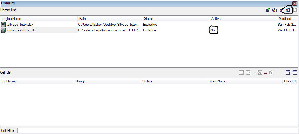
Notice that after
the pcells library is activated we can see the listing of the cells in
the
bottom of the window.
Close this window.
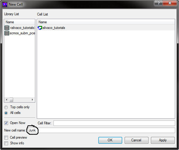
Let's create a new
cell called "Junk" using Cell -> New.
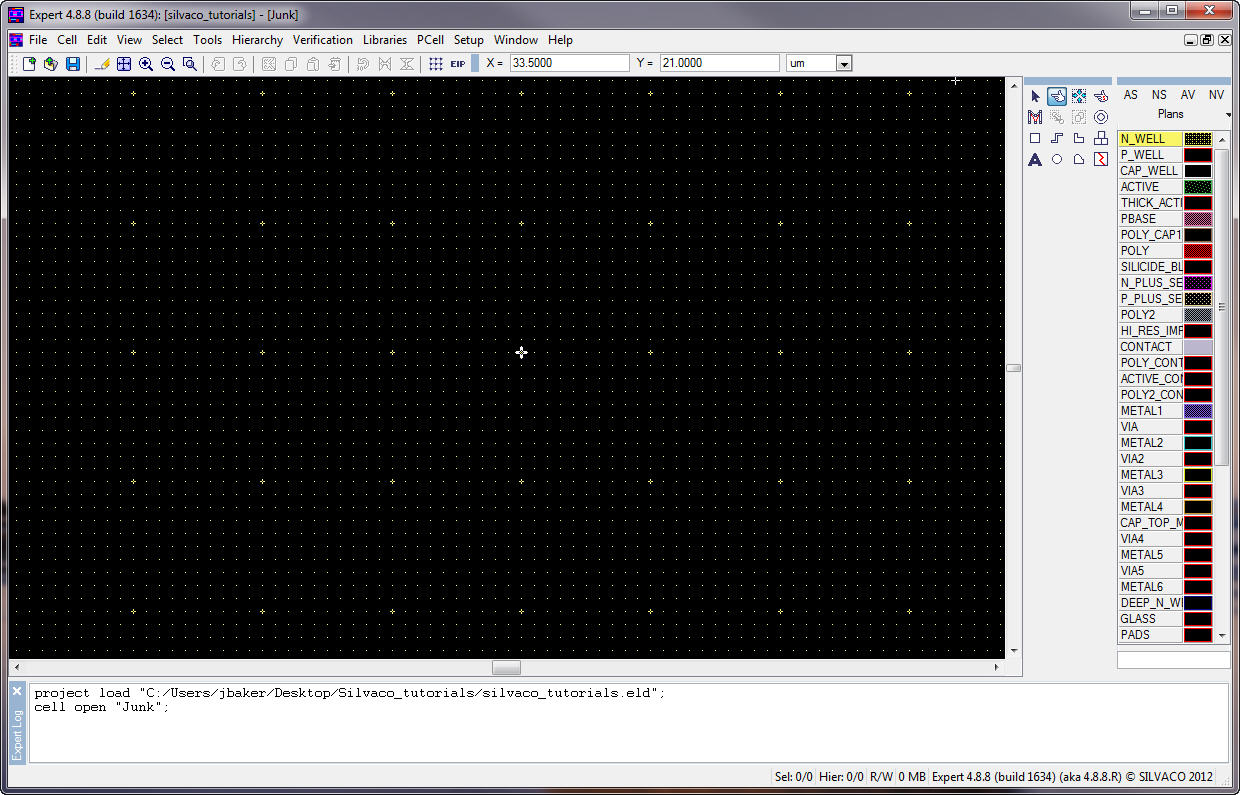
After using the
menu commands View -> Filling -> Stipple
and re-sizing the windows
we get the following.
To avoid having to
repeat this command, as the author did in the video, whenever you open
a new
cell simply use Setup -> Save Setup menu
items.
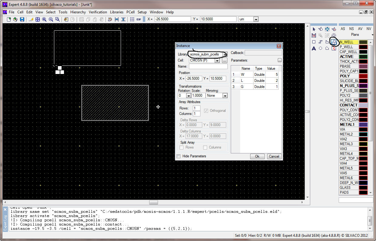
In this
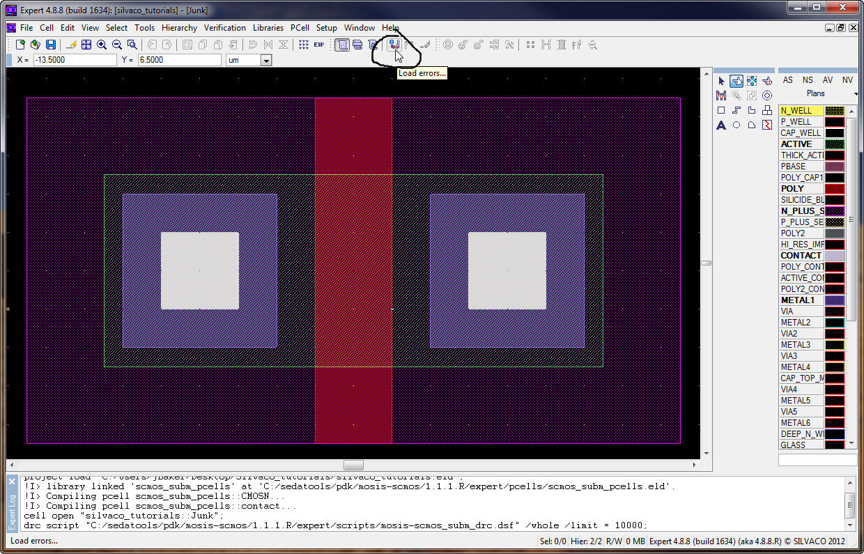
"Junk" cell let's place an instance of the CMOSN cell by clicking on
the circled icon on the RIGHT below.
Move the Instance
window, re-size it, and then select the "scmos_subm_pcells" library
and the CMOSN cell.
In the drawing
click the LEFT mouse button to place the instance of the CMOSN cell.
Note that the
"(P)" following the name indicates that the cell is a parameterized
cell, that is for example, changing the parameter W or L will change
the cell's
layout.
After
instantiating the CMOSN cell hit Cancel and the F
(to fit the cell in
the window).
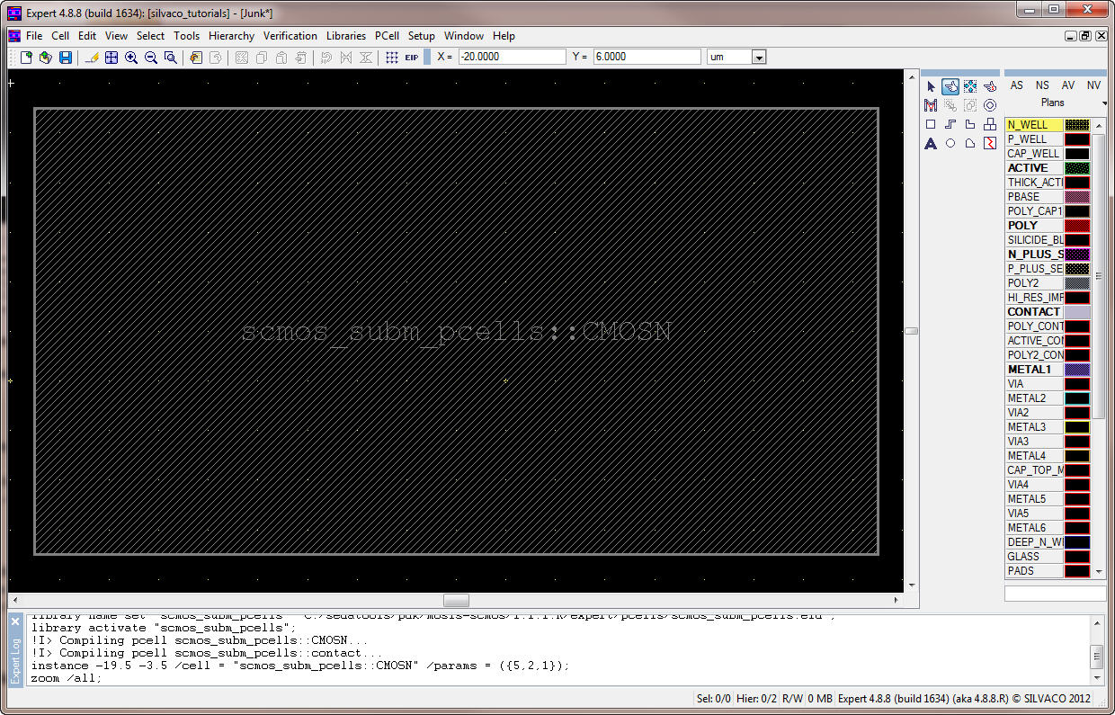
Before going any
further save the setups, Setup -> Save Setup,
and save the expert
layout design project file, silvaco_tutorials.eld, using File
-> Save
(CTRL+S)
Looking at the
above results we can't see what is inside the cell.
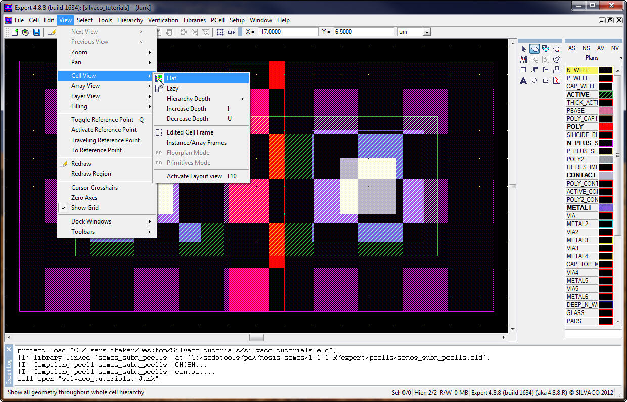
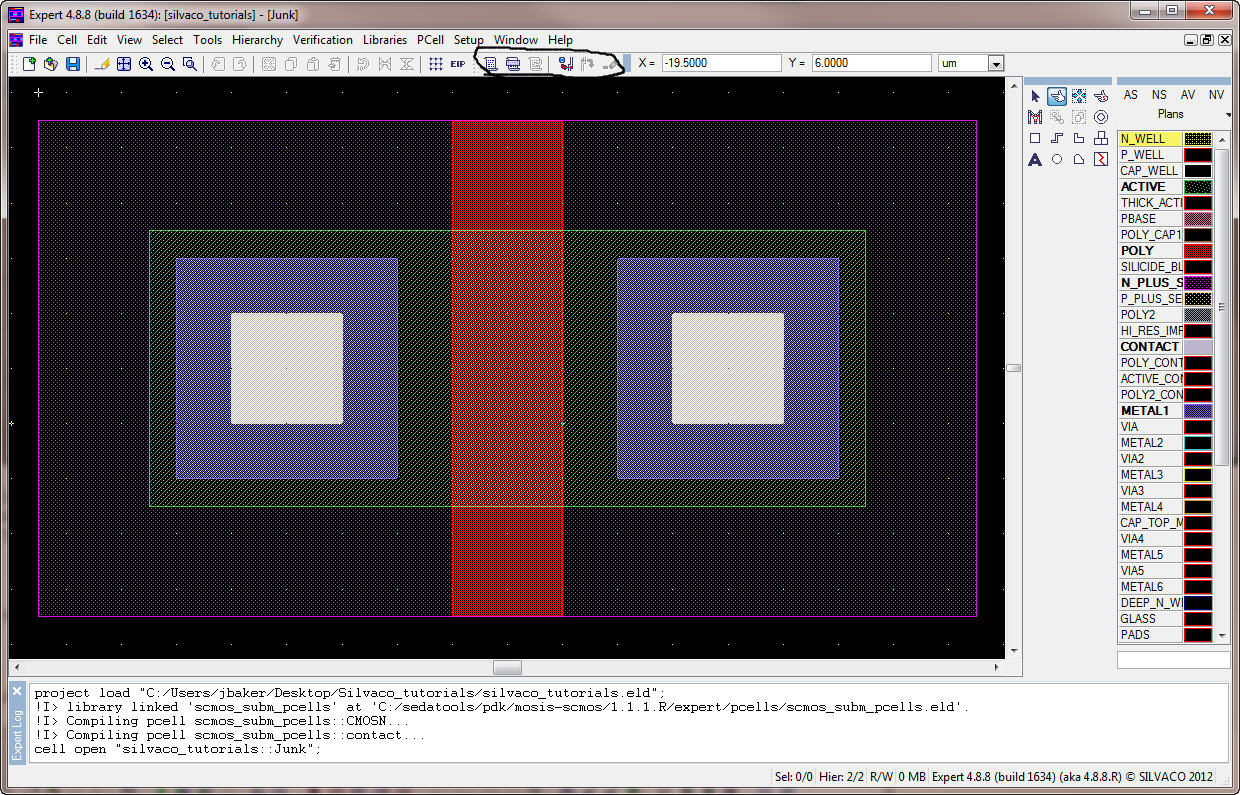
Use View
->
Cell View -> Flat to show the contents of the cell.
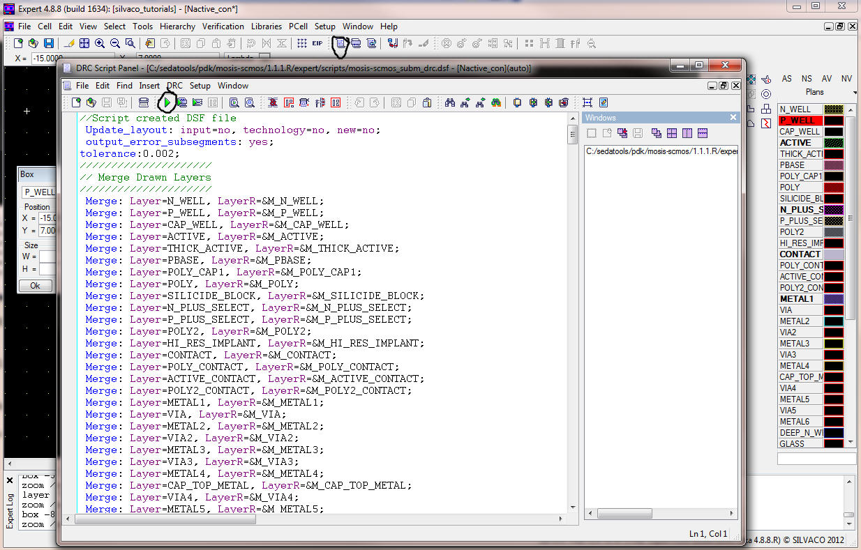
Let's now design
rule check (DRC) this layout.
Go to View
-> Toolbars -> DRC to show the DRC tool bar
(below).
Then select the
DRC script panel using the ![]() icon.
icon.
Next use File
-> Open and navigate to the mosis-scmos_subm_drc.dsf
design rules as
seen below.
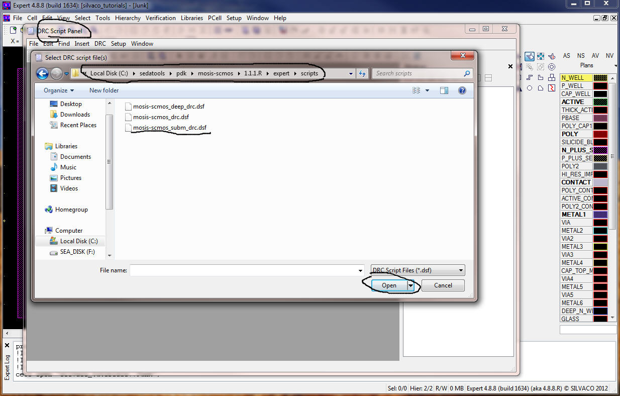
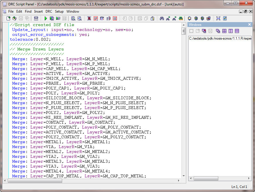
After hitting the
Open button we get the following.
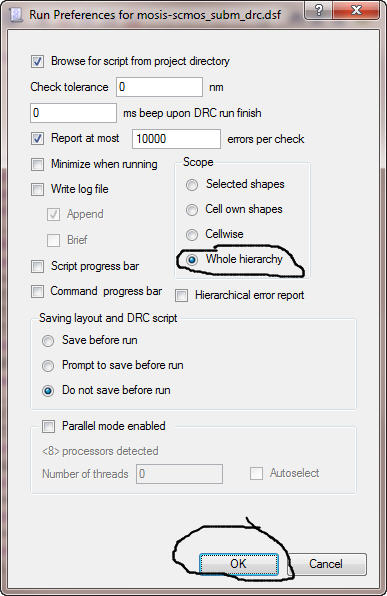
Next select the
menu Setup -> Current DRC script run preferences...
Select the Scope
to be the "Whole hierarchy" (DRC everything in the cell) and hit OK.
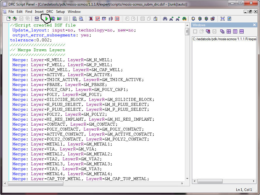
Next, hit the Run
button on the DRC Script Panel.
 .
.
Close the DRC
Script Panel.
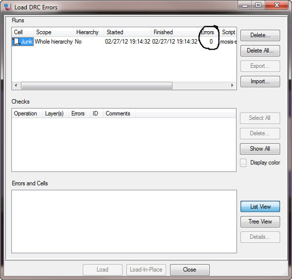
Load the DRC
errors.
There aren't any
errors, as seen below, so let's create some.
Close this window
and return to the Expert window.
Press - (the minus
key) to zoom out.
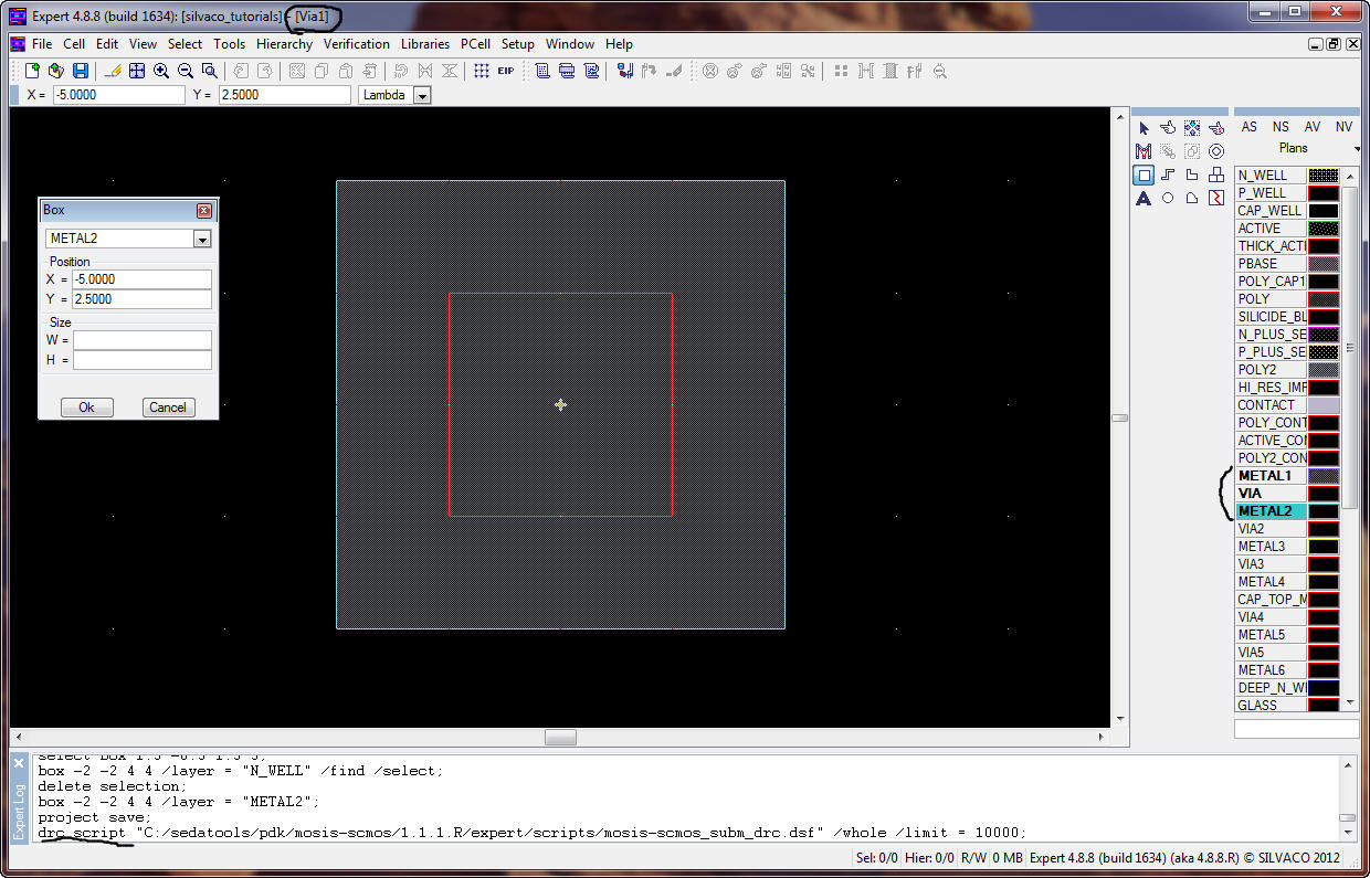
Next select the
METAL1 layer (click on the color, not the name, on the RIGHT) and the
Create Box
icon (circled below).
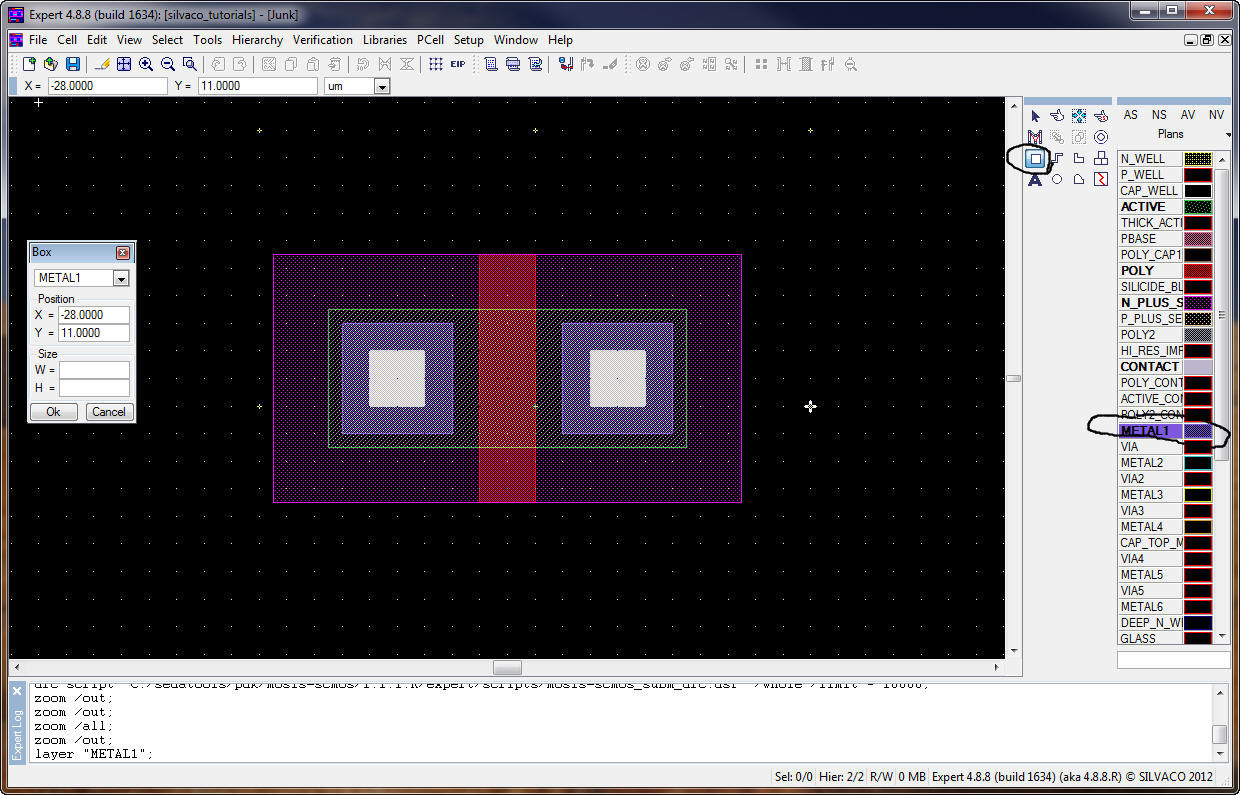
Add a box as seen
below.
Use F
to
fit the layout to the drawing area.
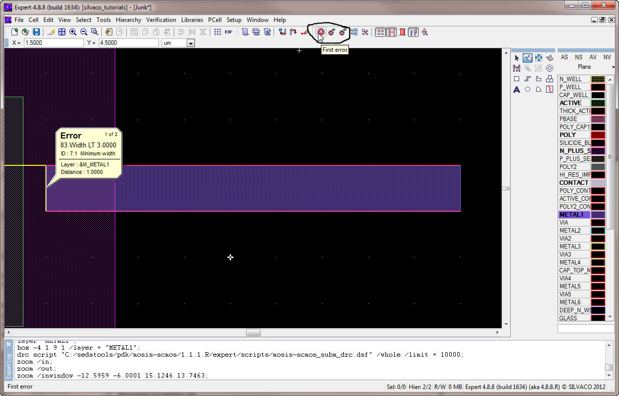
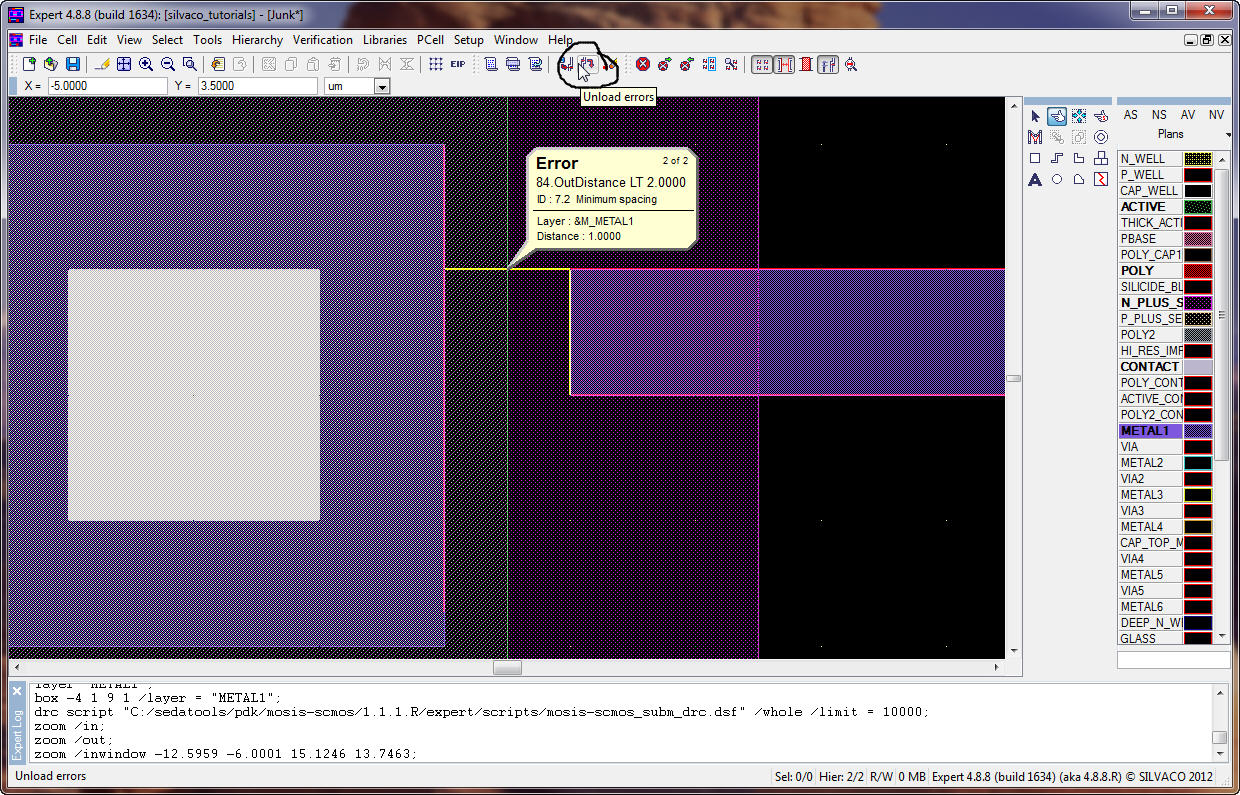
The box is drawn
on the METAL1 layer and violates two design rules, spacing and width
(rules 7.1
and 7.2 as seen in SCMOS design rules).
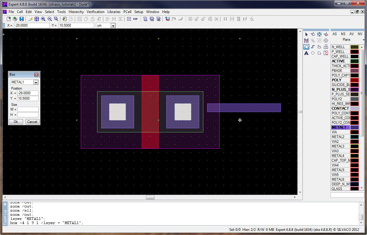
Follow the
procedures given above DRC the layout again.
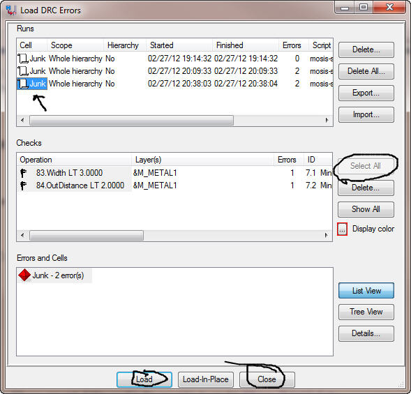
After running the
DRC, select the last Run, then Select All (errors), then Load followed
by pressing
Close.
The image seen
below shows how the DRC errors are displayed, icons for the Show all
errors and
Wireframe error marks.
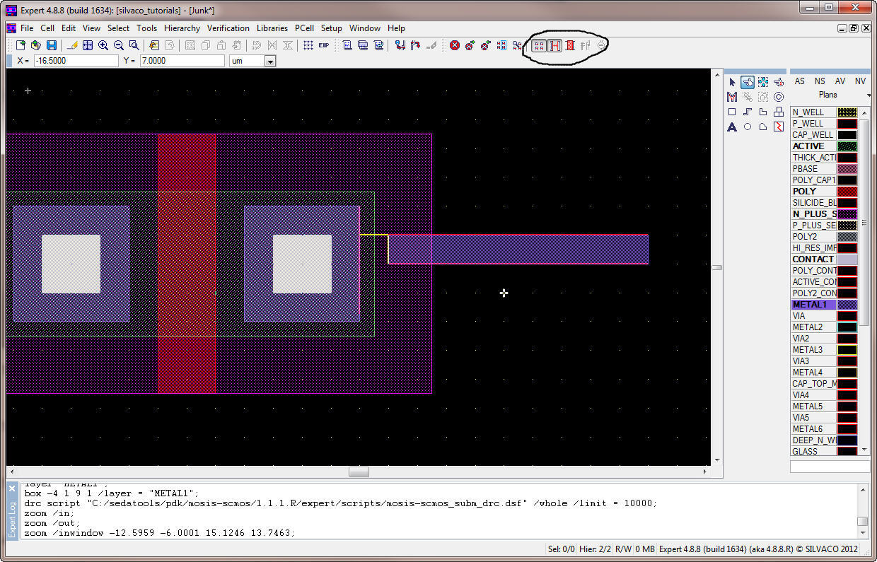
To step through
the errors use the icons seen circled below.
To stop looking at
DRC errors use the Unload errors icon seen below.
At this point
running a DRC and looking at the results should be understood.
Use File
-> Save
to save the expert layout design file, that is, silvaco_tutorials.eld.
Also, go ahead and
close the cell named "Junk".
Next let's create
cells called Nactive_con, Pactive_con, Nwell_con, and Psub_con for
making
metal1 connections to the n-active, p-active, n-well, and p-substrate
respectively.
In a process
specific PDK these (parametric) cells (pcells) will already be laid
out.
However, in these
generic SCMOS setups they aren't available.
Before laying
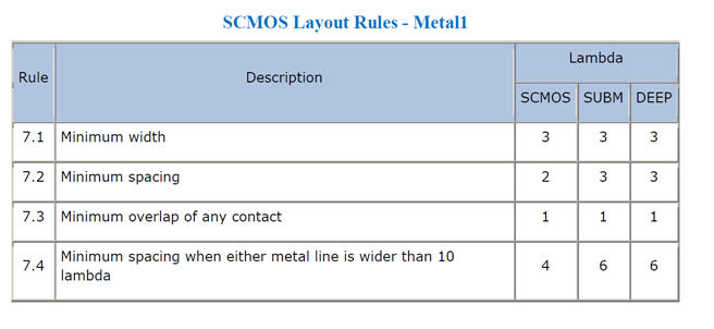
these cells out let's review the SCMOS
rules and show, below, the design rules related to metal1, contact,
active,
wells, and p-/n- selects.
For the ACTIVE
Layer
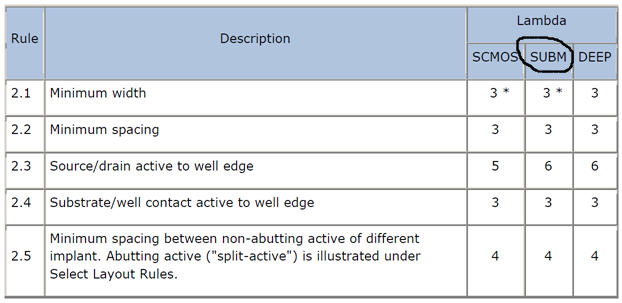
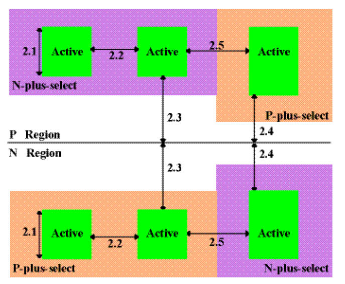
For the CONTACT
layer.
For the SELECT
layers.
For the METAL1
layer.
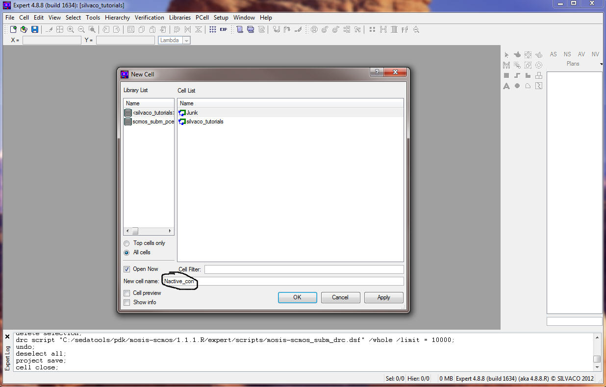
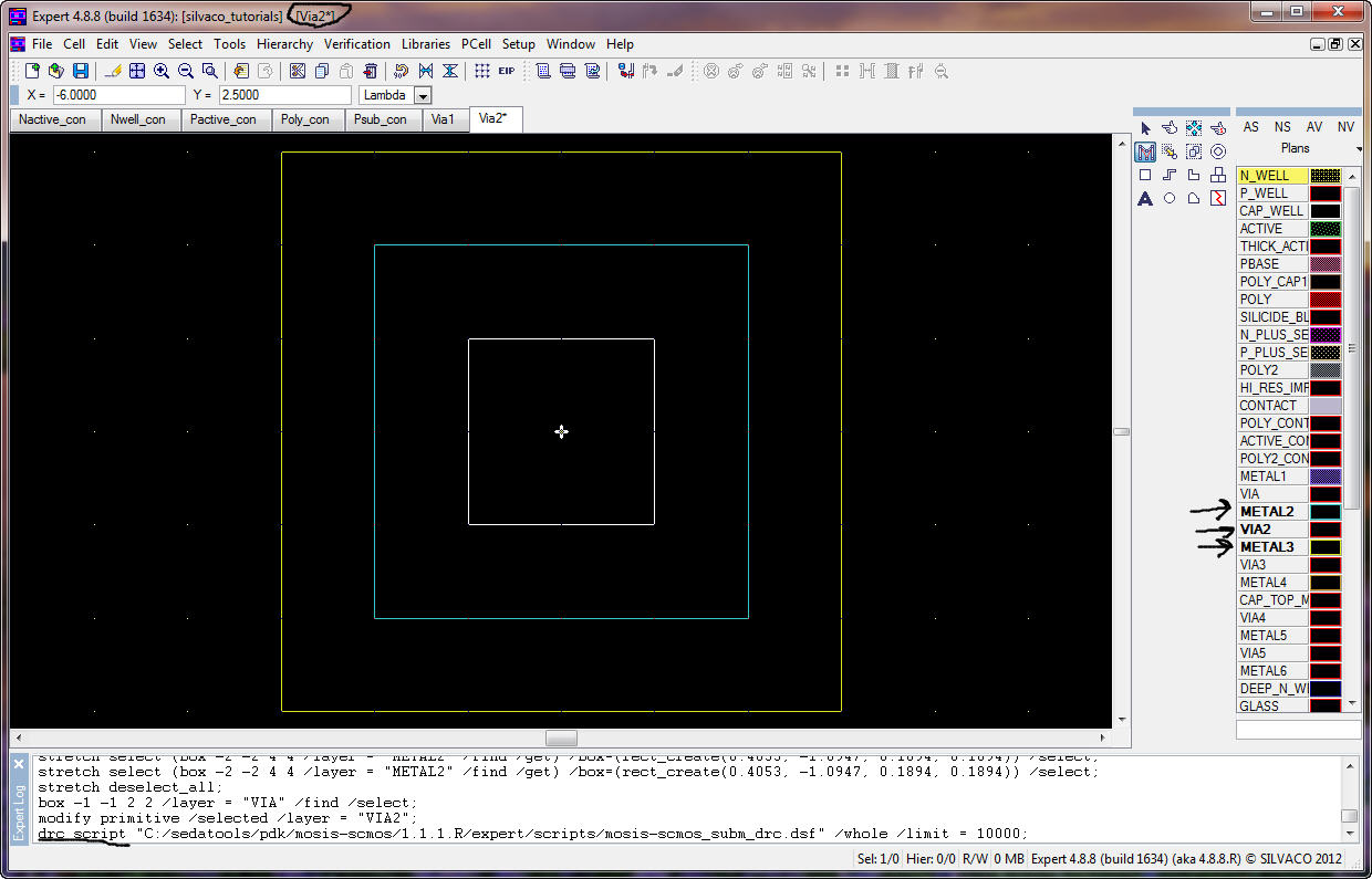
To begin, create a
new cell called, Nactive_con.
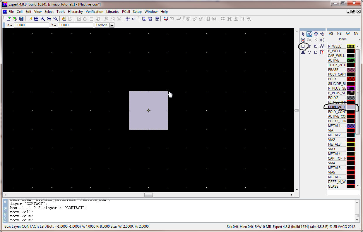
Create a 2 Lambda
by 2 Lambda box on the CONTACT layer.
Note that the
minus key, -, and the F
key were used to fit and zoom out.
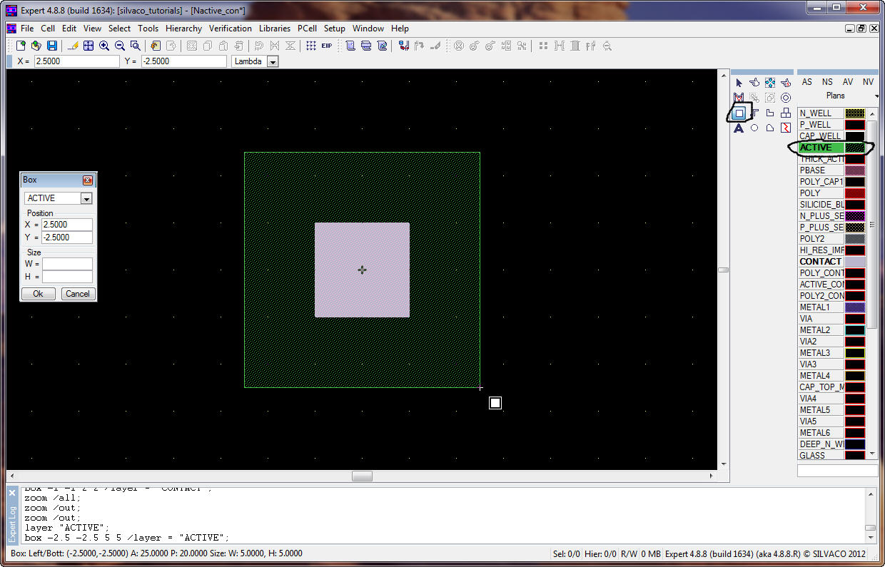
Next draw a box on
the ACTIVE layer that is 5 by 5 centered around the contact.
Notice, below in
the RIGHT layer menur, that the layers used in the cell are BOLD.
Then draw a box on
the METAL1 layer that is 4 x 4.
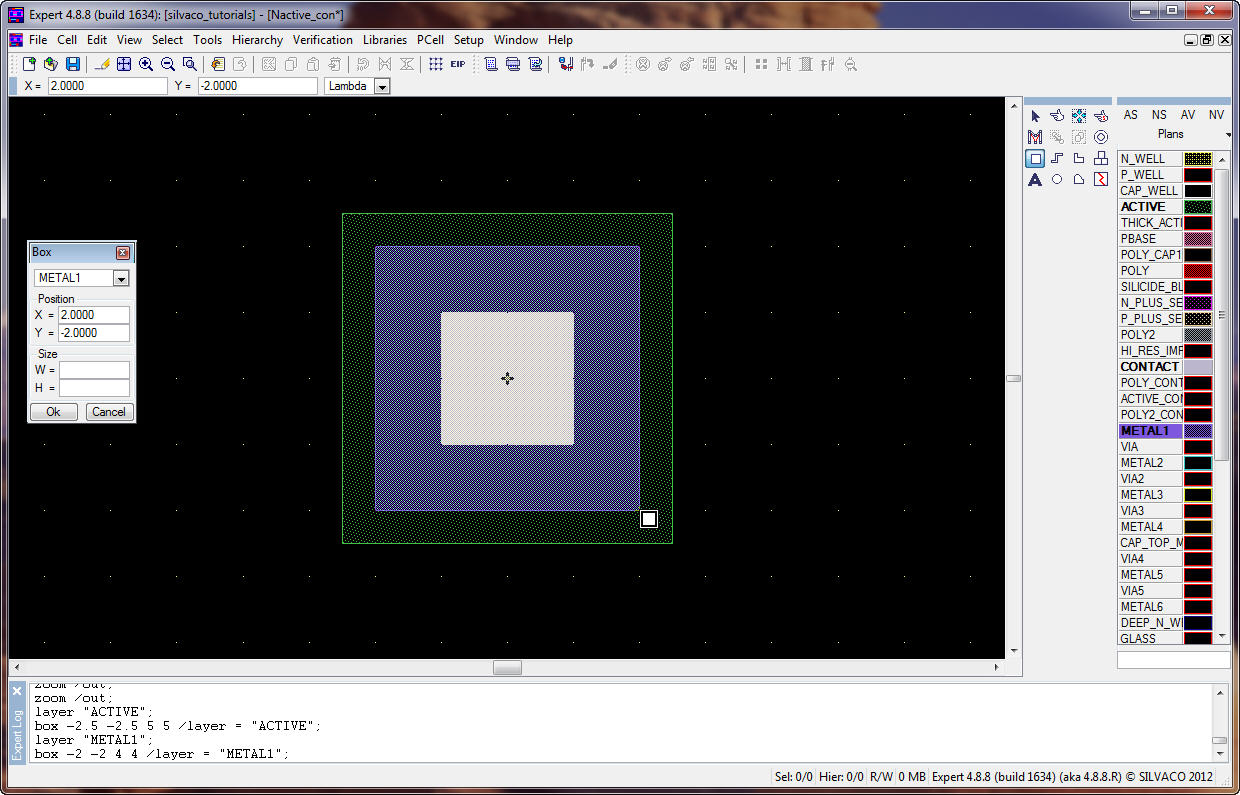
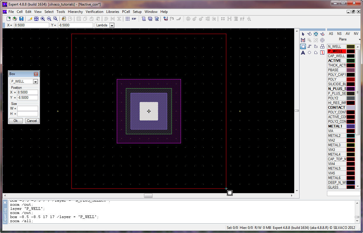
Next add a 7 x 7
box on the N_PLUS_SELECT Layer and a 17 x 17 box on the P_WELL layer.
Note that there
isn't a p-well in the C5 process; however, we draw it here to make the
layouts
more generic.
Let's DRC this
layout.
Load the DRC
errors.
Select the last
Run, Load the errors, then Close the window.
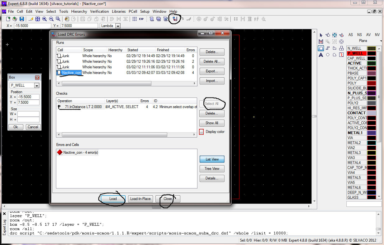
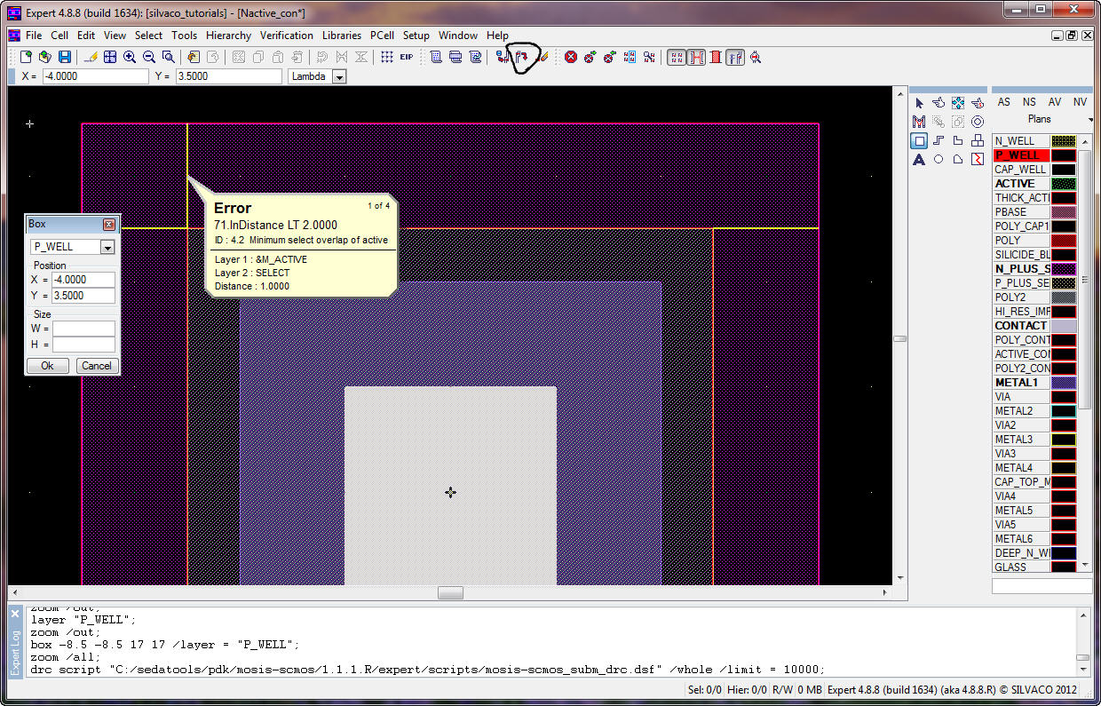
There are 4 errors
that all have to do with the N_PLUS_SELECT layer not overlapping the
ACTIVE
layer by at least 2 (the overlap is 1.5 below).
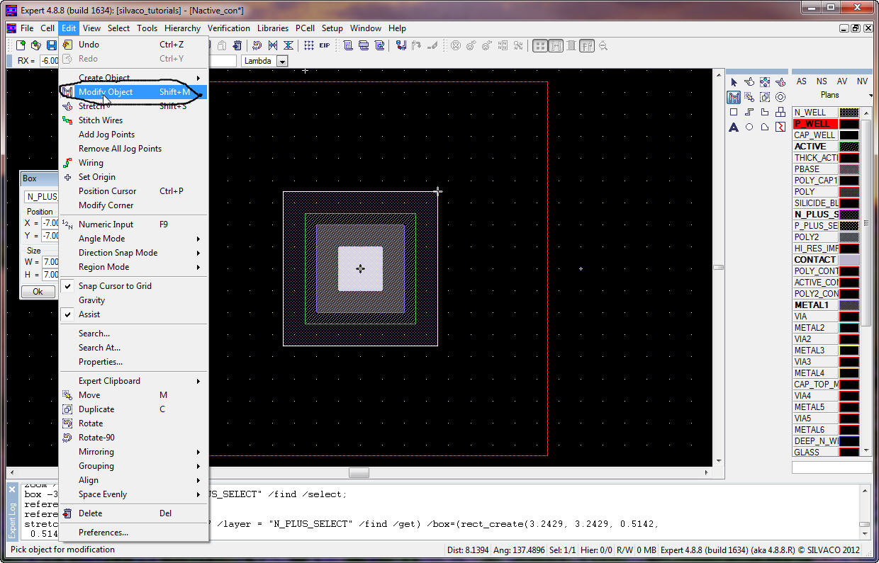
Unload the DRC errors
using the circled icon seen below.
Select the
N_PLUS_SELECT layer then Edit -> Modify Object (or
Shift+M or the
icon on the RIGHT menu)
Re-size the box
either using the mouse or the smaller window on the LEFT side of the
image
below.
DRC the below
result to ensure that there aren't any errors (there shouldn't be).
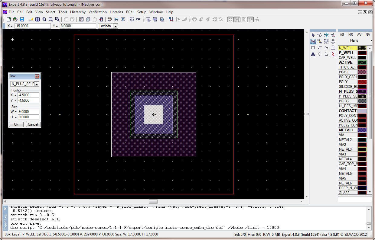
Save the
silvaco_tutorials.eld file.
Then do a Cell
-> Save Cell as... and save the Nactive_con cell as
Pactive_con.
Select the
N_PLUS_SELECT box and change it (Edit -> Modify Object or
Shift +
M) to P_PLUS_SELECT
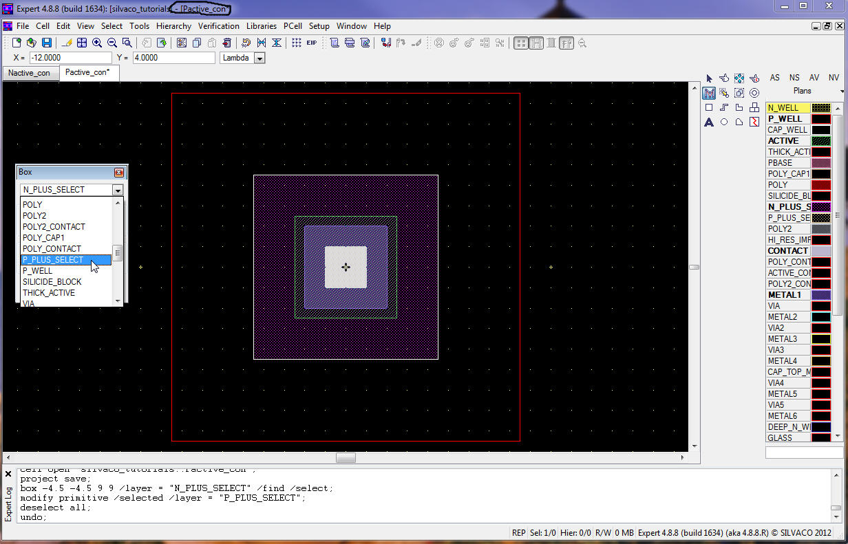
Then select the
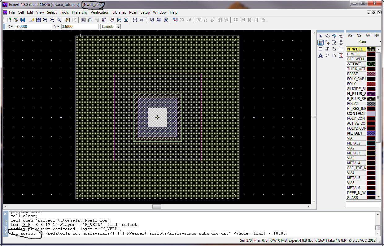
P_WELL box and change it to N_WELL.
Save the layout
and DRC the Pactive_con cell, below, to ensure no DRC errors.
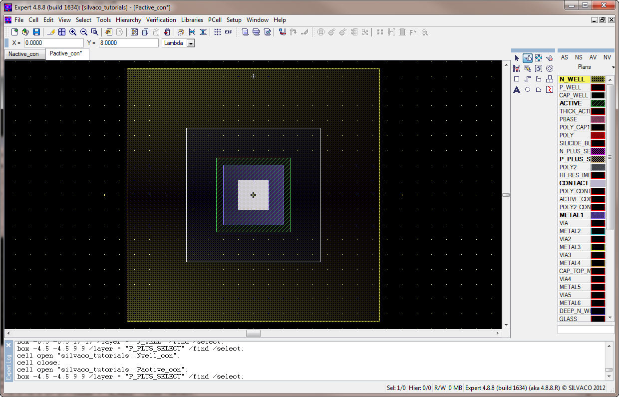
After saving the
*.eld file (the layouts) save the Pactive_con cell as Psub_con (Cell
->
Save Cell as...) and save the Nactive_con cell as Nwell_con.
In the Nwell_con cell
change the P_WELL layer to N_WELL and DRC, below.
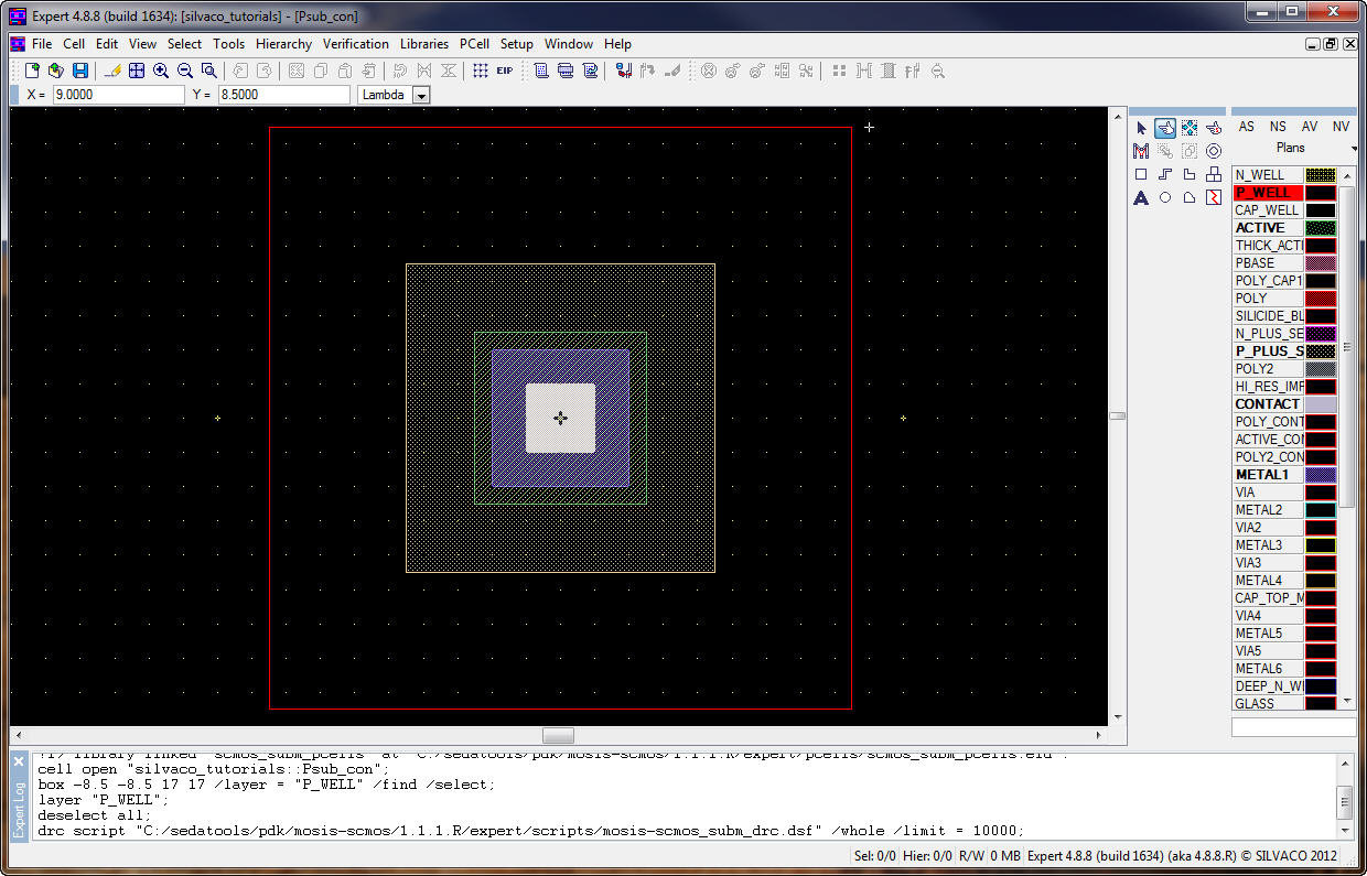
Then, in the
Psub_con cell, change the N_WELL layer to P_WELL and DRC.
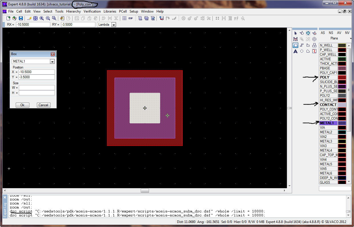
Before quitting
let's lay out, and DRC, a few more cells.
Note that to move
an object you select it then press M, see the Edit
menu.
Also, above the
layers menu are some selections that may be useful, AV
is all visible, NV
is none visible, AS is all selectable, and NS
is none selectable.
Right clicking on
the color of a layer will allow you to, for example, make only that
layer
selectable right after pressing the NS.
This ends our
second tutorial.
For your reference
the final contents of the Silvaco_tutorials folder used in this
tutorial is
located in Silvaco_Tutorial_2.zip.