Silvaco EDA Tutorials from
CMOSedu.com
Tutorial
1 – Getting started, drawing an inverter and simulating
Background
information
These tutorials will
introduce you to
Silvaco’s set of IC CAD tools for chip design. To
demonstrate the operation of the
tools we’ll
set them up for
(SCMOS) submicron design rules.
The
scale (lambda) for the
C5 process using the SCMOS rules is 300
nm and the technology
code is SCN3ME_SUBM (info).
This tutorial
assumes that the Silvaco IC CAD tools are installed on your computer
and that
the SCMOS Design Kit has been installed,
see the download
link at the bottom of the page seen here.
The tools used in
the SCMOS Design Kit include:
Gateway for schematic entry
SmartSpice for circuit simulation
SmartView for viewing
simulation results
Expert for layout
Guardian DRC for design rule
checking (DRC)
Guardian LPE for layout parameter
extraction (LPE)
Guardian LVS for layout versus
schematic (LVS) checking
Parasitic
Extraction with HIPEX-C/R/RC
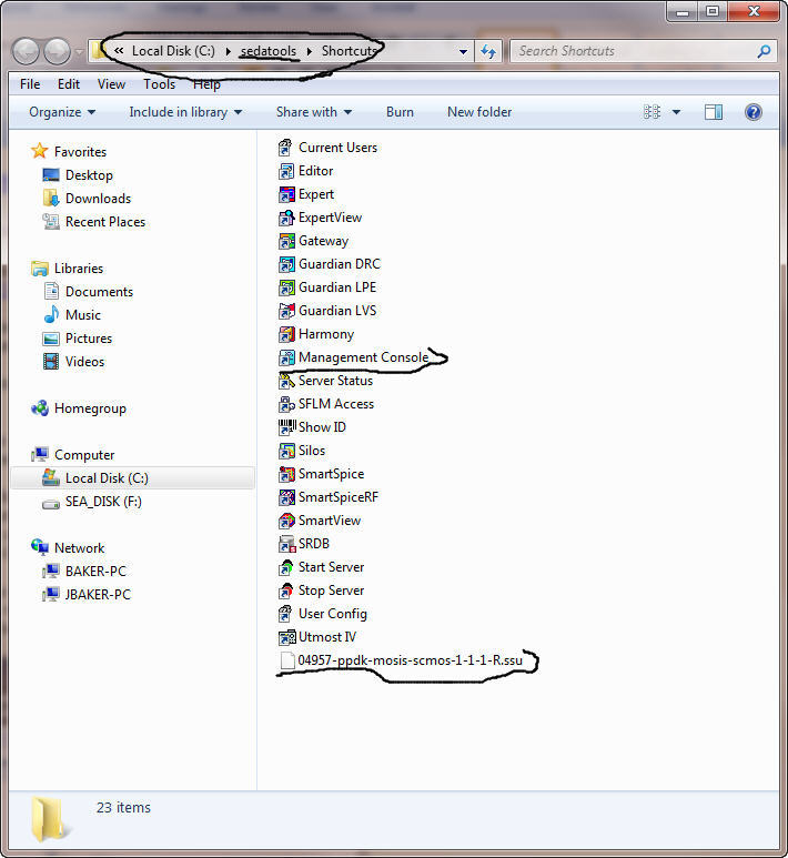
Other tools that
may be used in a specific process design kit (PDK) are seen in the
Silvaco EDA
(electronic design automation) Tools
(sedatools) shortcuts folder seen
below.
Note the *.ssu
file at the bottom which is the setup file for the MOSIS SCMOS PDK
(installed
per directions using the Management
Console also seen
below, link).
Let's begin the
first tutorial.
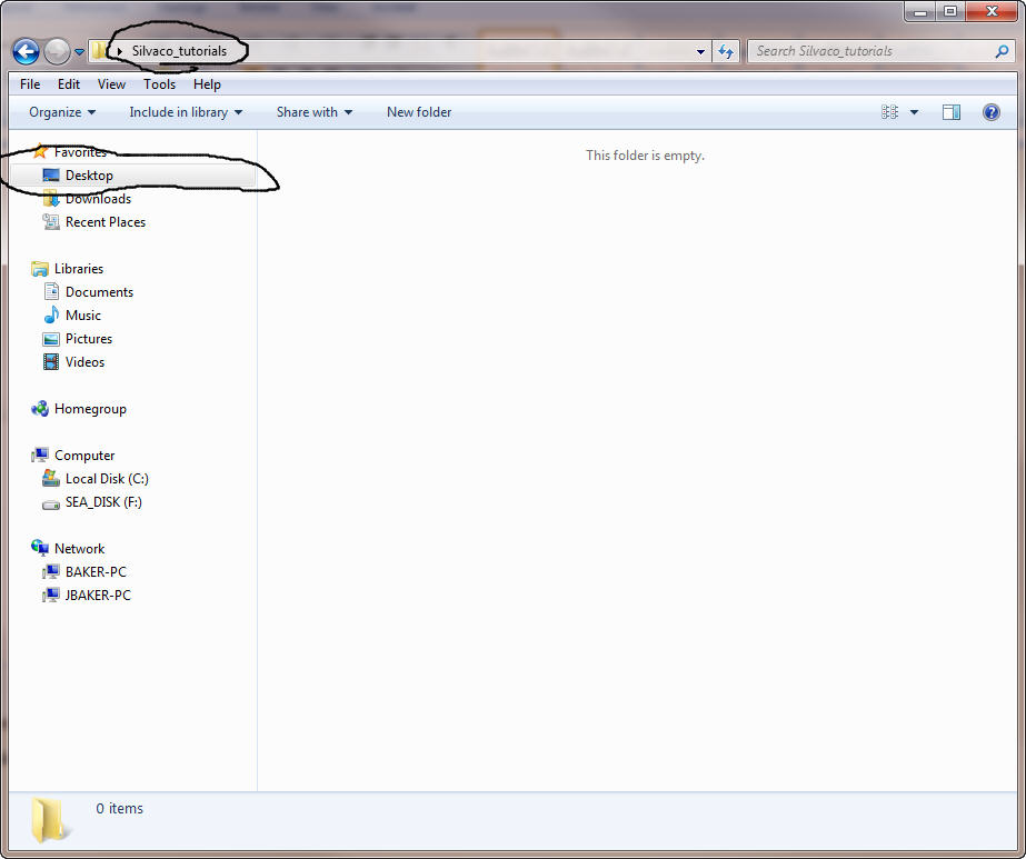
Assuming that the
Silvaco EDA Tools and MOSIS PDK are installed on your computer begin by
creating a folder on your desktop called Silvaco_tutorials.
We’ll place all of
the work from these tutorials in this folder.
Let’s draw a
schematic of an inverter. To start, double click on the Gateway
icon seen above in the sedatools Shortcuts folder.
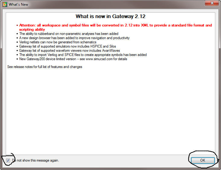
The following
information will appear.
Select “Do not
show this message again.” (unless you want to see the message next time
you
start Gateway) and then OK.
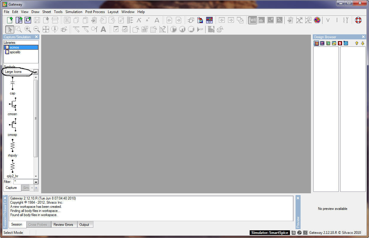
The Gateway
window is then seen below (after re-sizing to make smaller for this
tutorial).
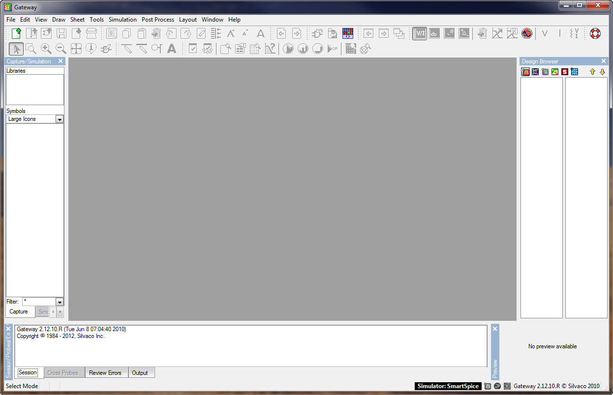
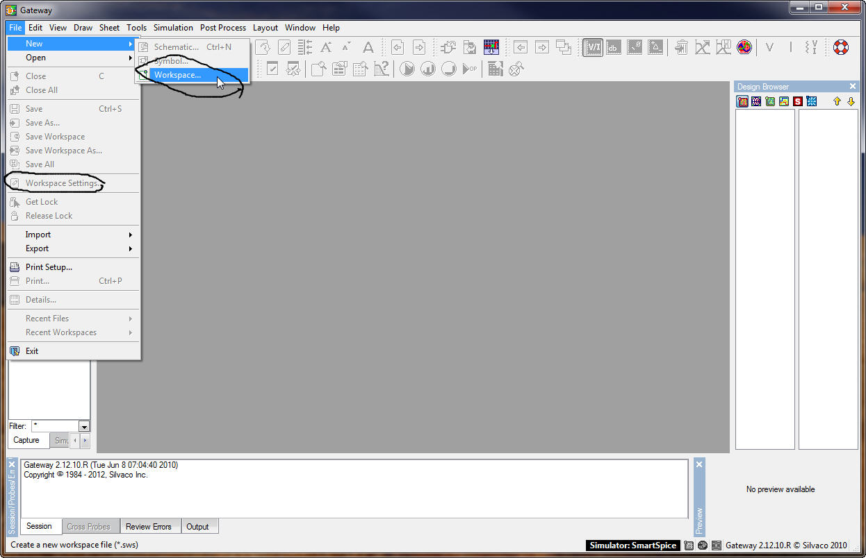
To begin we need
to tell Gateway the libraries we’ll
use in this design.
We do this by
creating a new Workspace, see below.
If we are opening
an existing design we can use Open ->
Workspace.
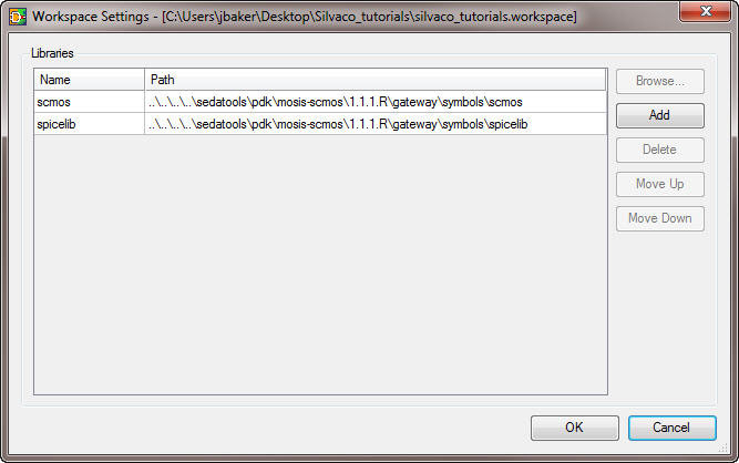
To view the
libraries specified in an open Workspace use the Workspace
Settings seen circled below.
Create the new
workspace in the Silvaco_tutorials folder you created on your desktop.
Call this
workspace “silvaco_tutorials”
as seen below.
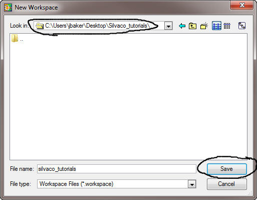
After hitting Save
the following will appear.
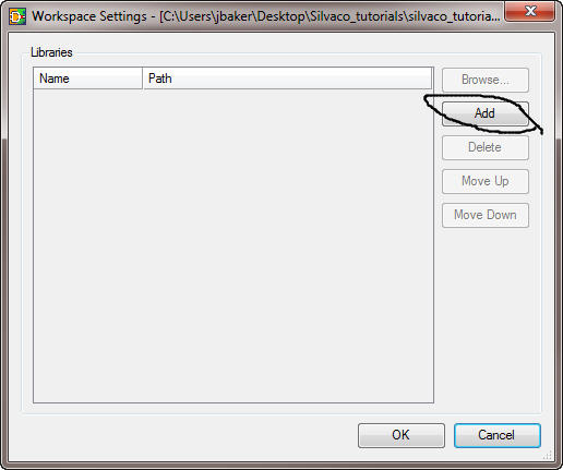
Click on the Add,
and then Browse, buttons to select the paths seen below.
Double click on “newlibrary” and change to the
names (scmos and spicelib)
seen below.
When finished
click on OK then, in Gateway, use File -> SaveWorkspace
to save the workspace.
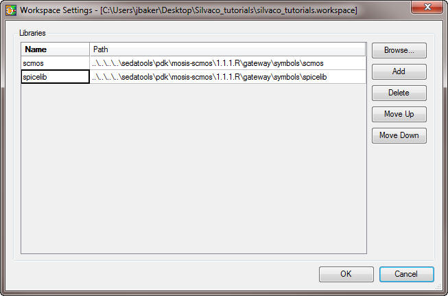
Now there is one
file in the Silvaco_tutorials folder on the desktop, that is, silvaco_tutorials.workspace
(verify this before going
further).
If you download
the Silvaco
IC CAD simulation examples from CMOSedu.com then, after
starting Gateway,
the first thing
you do (to view the examples) is open the specific chapter's workspace
file.
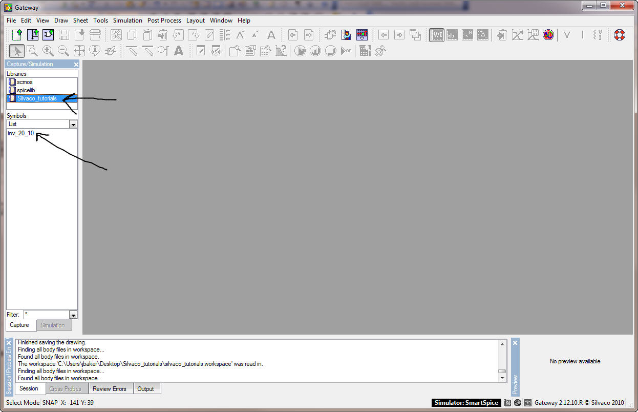
The Gateway
window will show the two
libraries on the left side as seen below.
Go ahead and
change how the symbols are displayed, e.g., large icons, list, etc. to
a view
you like (I like the "List" view).
Next use File
-> New -> Schematic or Ctrl+N
to create a new schematic.
Enter the name
seen below, an inverter using a PMOS with a width of 20 and an NMOS
with a
width of 10.
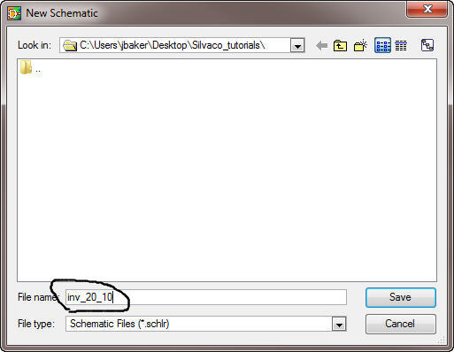
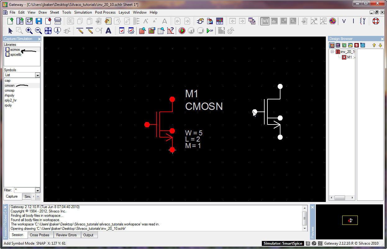
Select the scmos
library and the cmosn symbol.
Place, by clicking
in the drawing area, the symbol as seen below.
Use the menu View
-> Zoom Full (or, preferably, press the key F)
and View ->
Zoom Out (press -) to zoom out.
Next press the ESC
key to stop placing the cmosn symbol.
Next, we need to
set the MOSFET's width, length, and SPICE model name.
First, save C5_models.txt
(RIGHT click to save) to
the Silvaco_tutorials folder on your desktop.
Note, in this text
file, that the BSIM model names are NMOS and PMOS (easy to remember!)
Click on the
symbol to select it (the symbol turns from a red color to a green
color).
Then use Edit
-> Properties (or, preferably, just press q,
even though, below,
an uppercase Q is shown lowercase q works too) to change the MOSFET's
parameters.
Also,
double-clicking the LEFT mouse button the symbol edits the symbol's
properties.
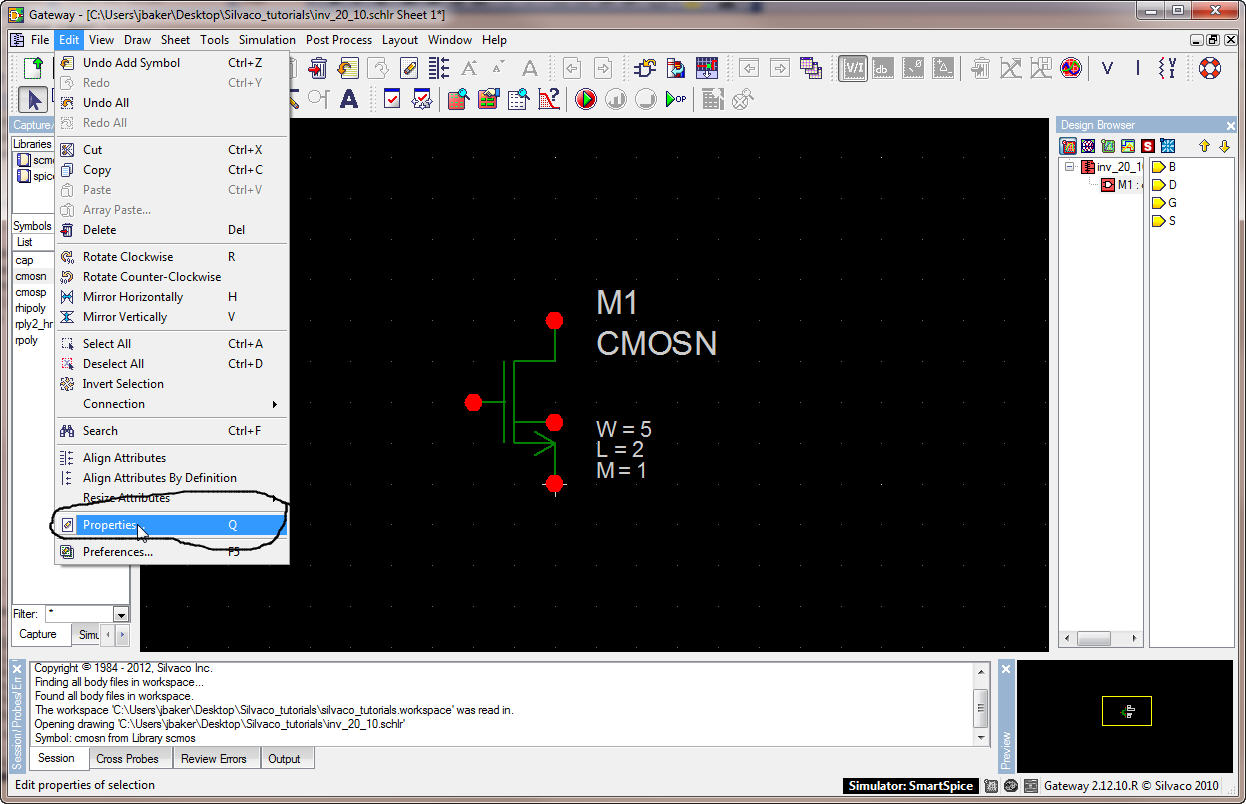
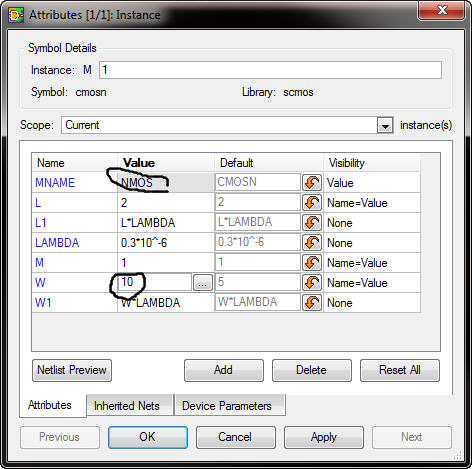
Change the SPICE
model name (MNAME) to NMOS and the width to 10 as seen below.
Again, as
mentioned near the top of the page, the
scale (lambda) for the C5 process is 300 nm and the technology code is
SCN3ME_SUBM (info).
Comment - M indicates the
number of MOSFETs in
parallel (most of the time this is 1) which results in an increase in
the
MOSFET's width to W*LAMBDA*M.
Select the scmos
library and the cmosp symbol (below).
Place the symbol
into the schematic as seen below and press ESC to stop placing the
symbol.
Hit F
to
fit to the window (or press the fit icon on the menu).
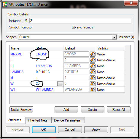
Next we need to
change the width of the PMOS to 20 and the SPICE model to PMOS.
Select the cmosp
symbol and press Q (or just double-click on the
symbol to edit the
symbol's properties).
After changing the
width to 20, as seen below, we try to change the spice model name to
PMOS
(however, we can't change CMOSP to PMOS).
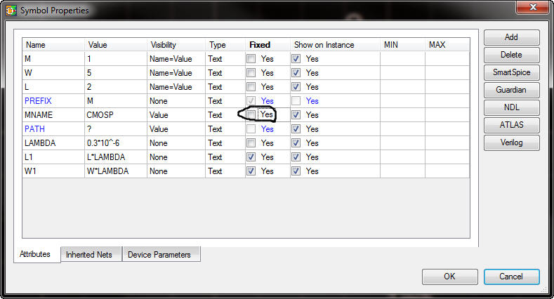
The value of MNAME
is fixed and we can't edit it (note that CMOSP is blue indicating it
can't be
changed).
To make MNAME
editable let's double click on the cmosp symbol name on the LEFT as
shown below
(or use the icon or use File -> Open -> Symbol or just
press N)
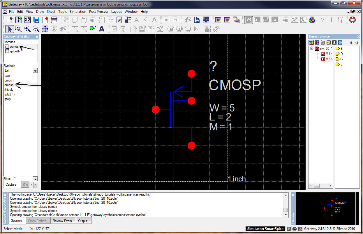
Next, with nothing
selected (click the mouse in an empty area), use Edit
-> Preferences
or simply press Q.
Then unckeck the
box that indicates that MNAME's value is fixed.
Comments - At this point we
could also change the
Value of MNAME to PMOS so we don't have to do that as we draw
schematics.
We could also
re-draw the symbol to replace the bipolar-derived symbols, see Fig.
4.14, with
CMOS symbols (no arrow since source and drain are interchangeable and
add a
bubble to the gate of the PMOS).
We could also use
the File -> Save As to make a 3-terminal MOSFET symbol version
(see examples
in the downloads at CMOSedu.com here).
Hit OK, then save
the symbol (File -> Save or CTRL+S)
then close the symbol (File
-> Close or simply press C).
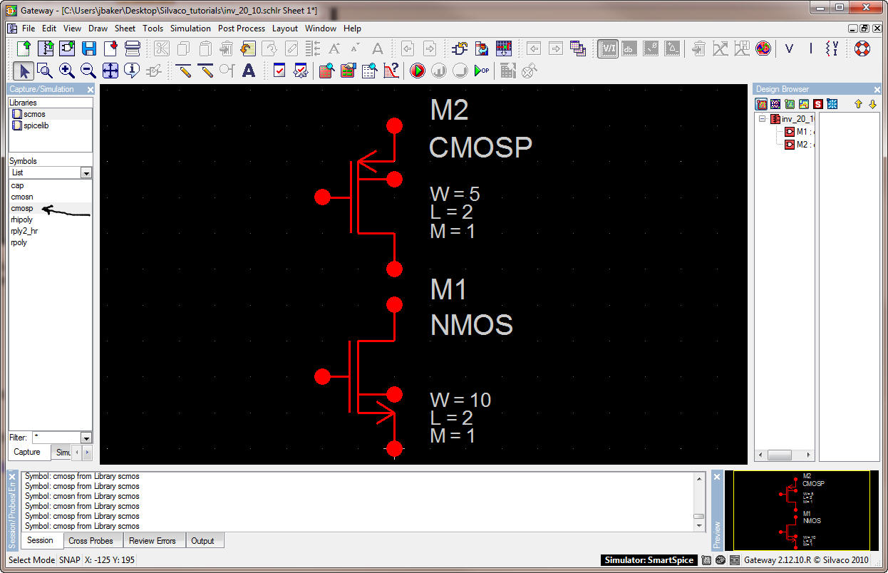
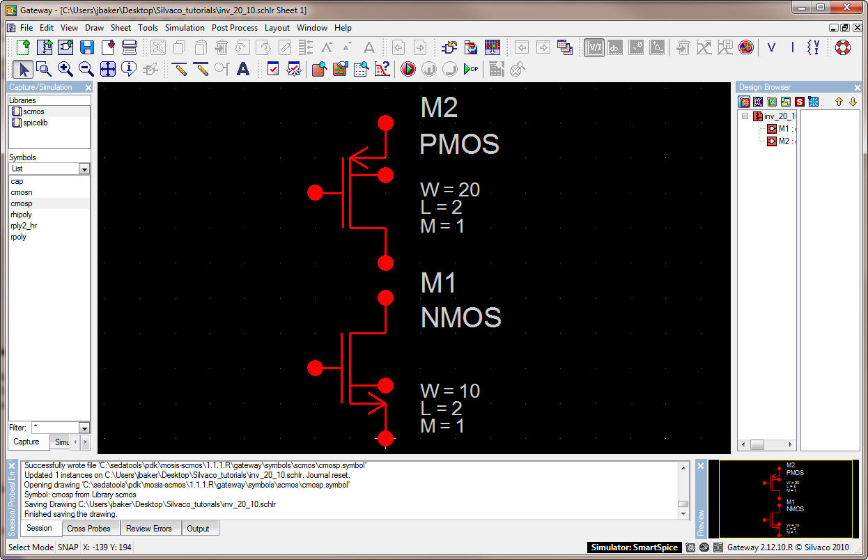
Change the PMOS's
model name to be PMOS as seen below and make sure the width is 20.
Save the
schematic.
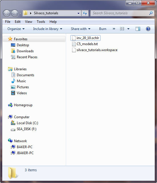
Let's take a quick
look at the contents of our desktop tutorial folder.
In addition to the
inverter schematic, we have the SPICE models and the workspace we
created.
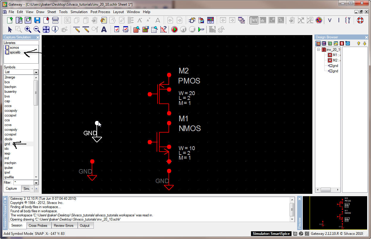
To simulate the
inverter we need to finish drawing it.
Select the
spicelib and add a couple of gnd symbols as seen below.
Use the -
(minus keyboard stroke) to zoom out.
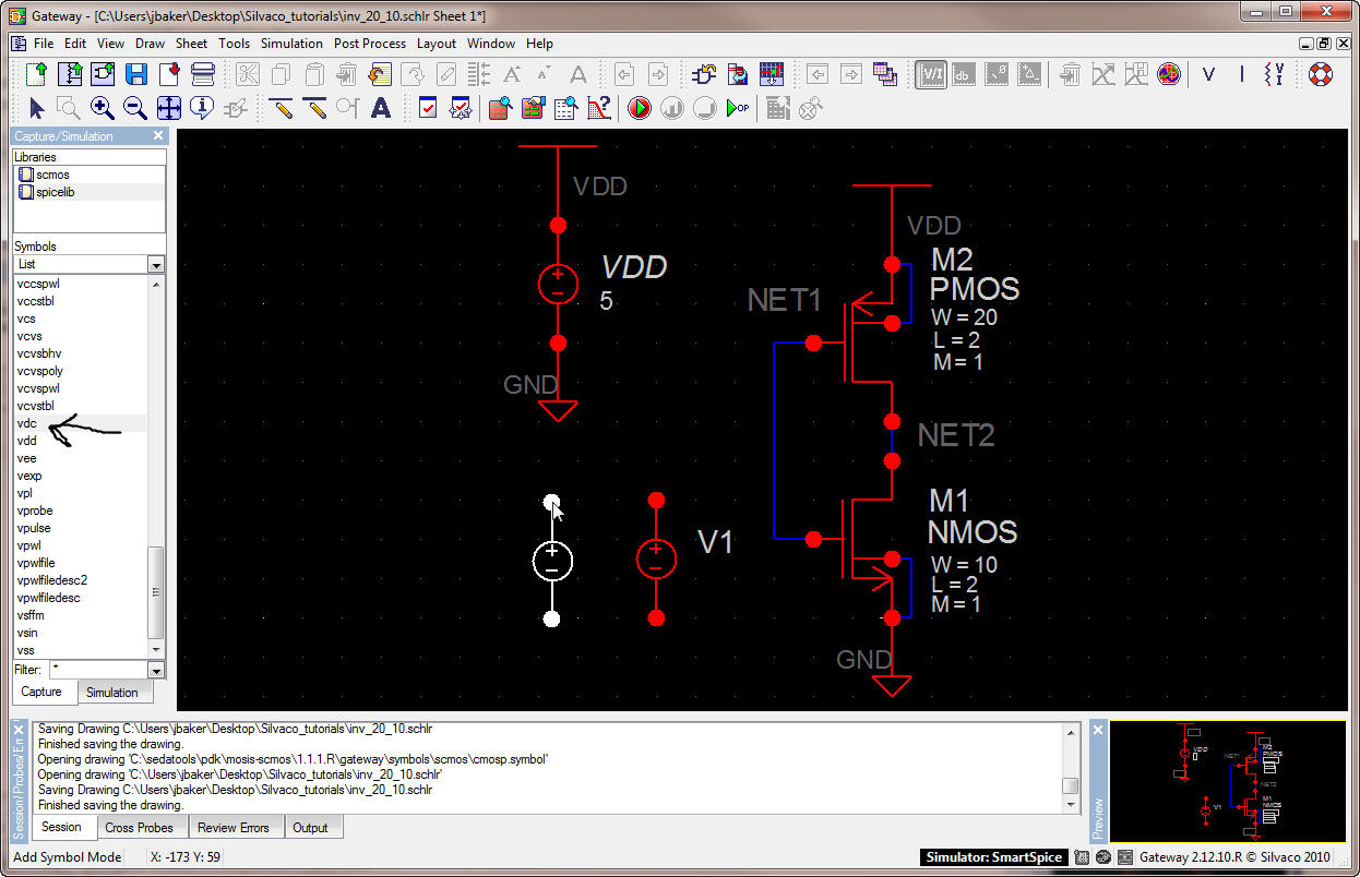
Next add the vdd
symbol (press ESC to leave the add mode).
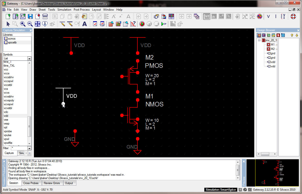
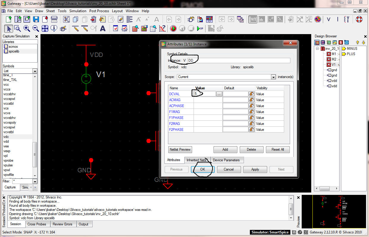
And finally add
the vdc symbol and rename it (double-click on the symbol or select it
and press
Q) VDD and set the DC value to 5.
Press OK.
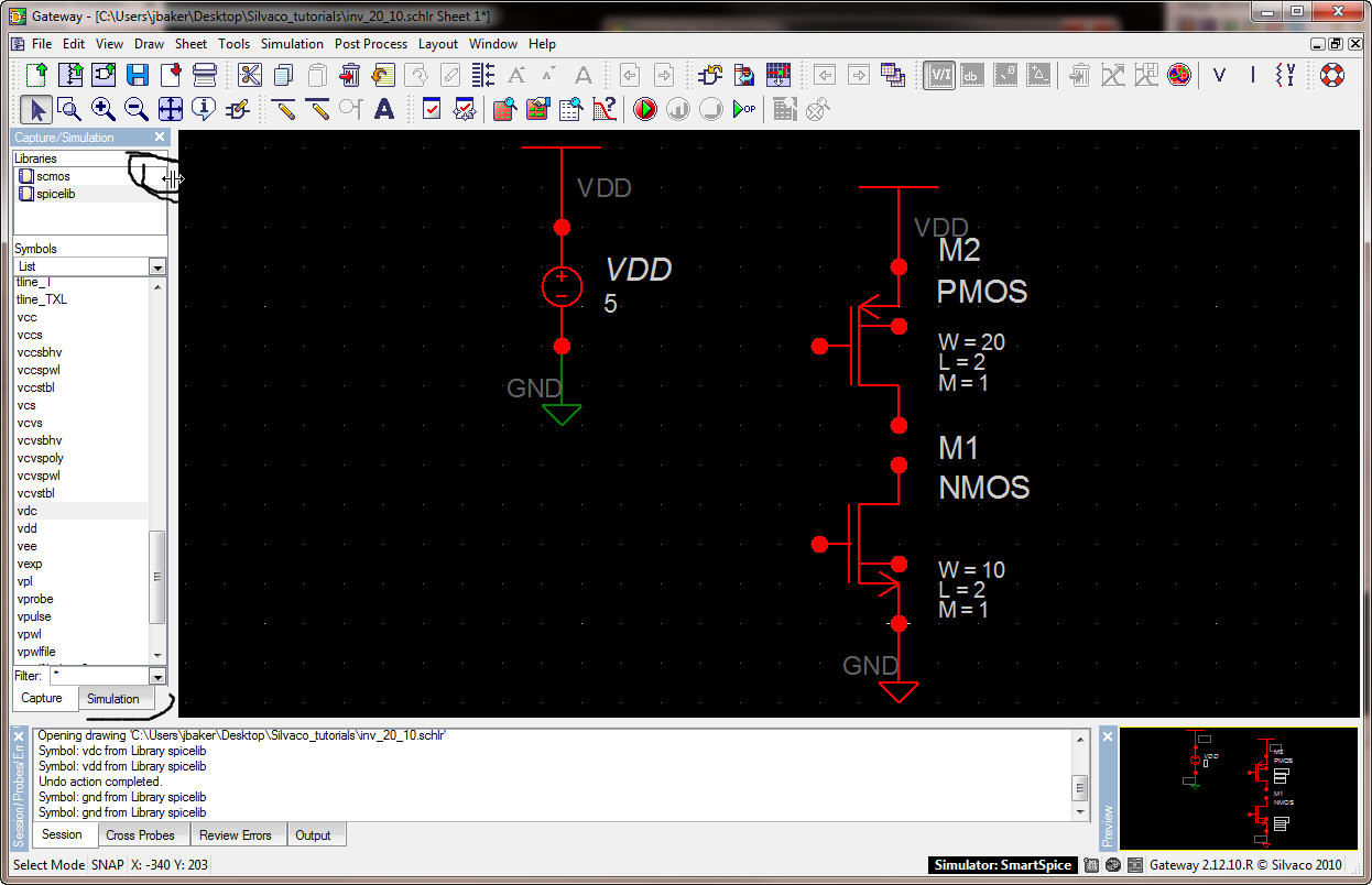
Let's give
ourselves a little more drawing space.
Close the Design
Browser window on the RIGHT and expand the Capture/Simulation window on
the
LEFT so that the Simulation tab on the bottom of the Capture/Simulation
window
is visible.
Move (click symbol
with the LEFT mouse button, hold, and drag) the gnd and vdc symbols to
the
positions seen below.
Hit F
to
fit the contents to the window and then save the schematic.
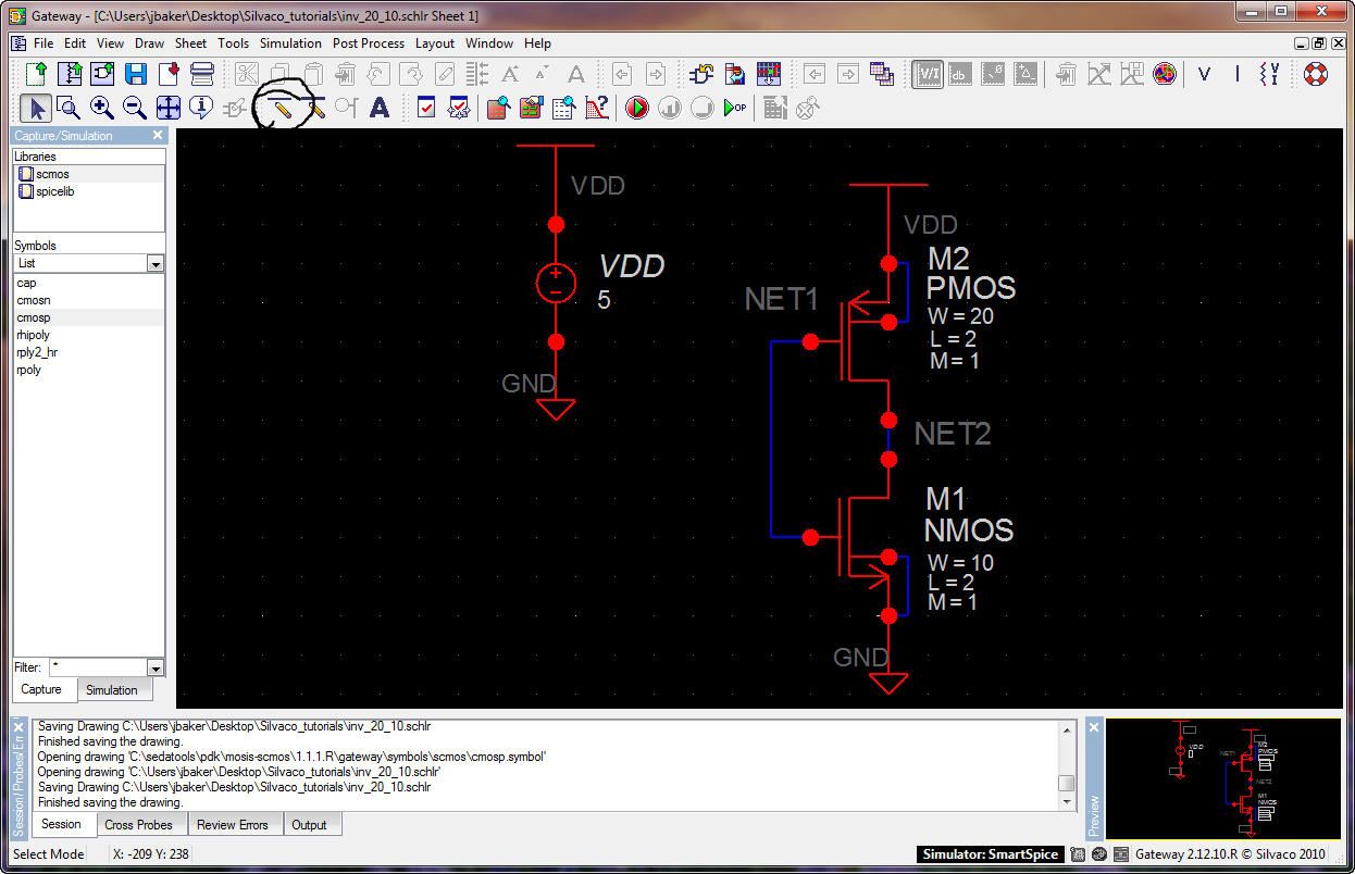
Next, let's draw
wires to connect the symbols together.
Press W
or
use the draw wire icon.
Re-arrange (move)
the MOSFET labels as seen below.
Don't forget to
connect the bodies of the MOSFETs to VDD and GND.
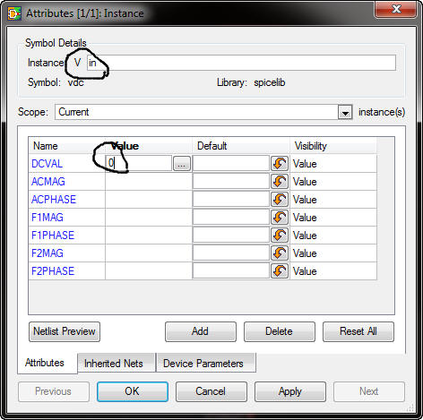
Next, add another
DC voltage source to the schematic.
Press ESC to exit
adding vdc then double click on the symbol.
Change the
instance name to Vin and set the value to 0.
Next add a gnd and
the wires seen below.
Double click on
the wire names NET1 and then NET2 and then change them to Vin and Vout.
Move the wire
names as seen below.
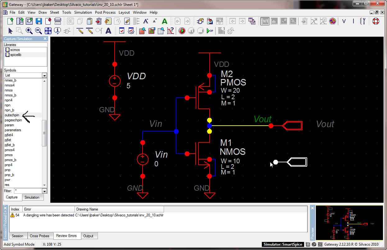
Finally, check the
schematic for warnings and errors by pressing the circled icon seen
below.
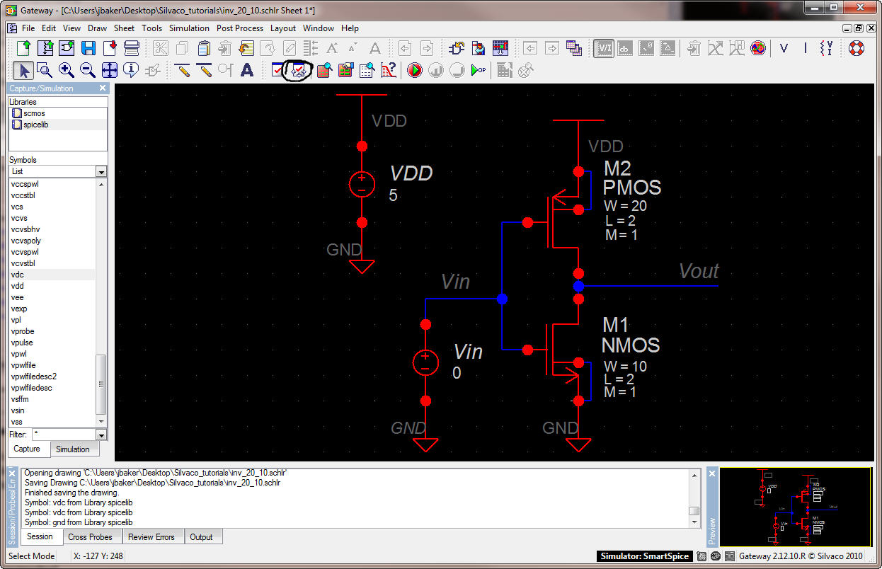
Checking the
schematic results in one warning, seen below.
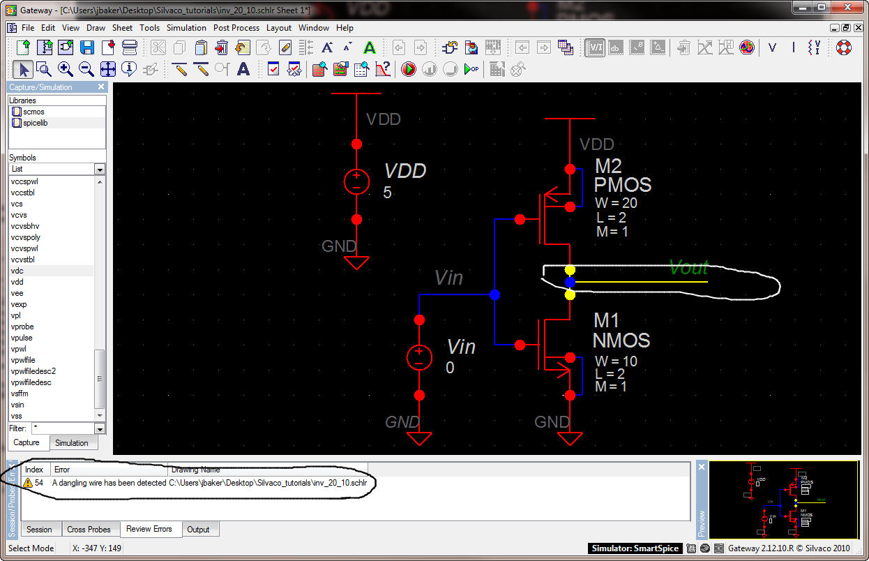
We can ignore this
warning, a dangling wire, which is fine or we can fix it by connecting
the
dangling wire to an output schematic pin symbol (outschpin) as seen
below.
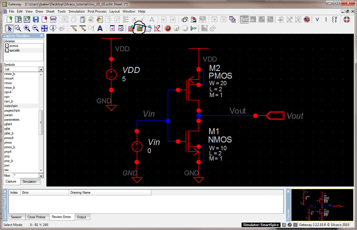
After moving the
Vout labels we get the following.
We are about ready
to simulate the inverter.
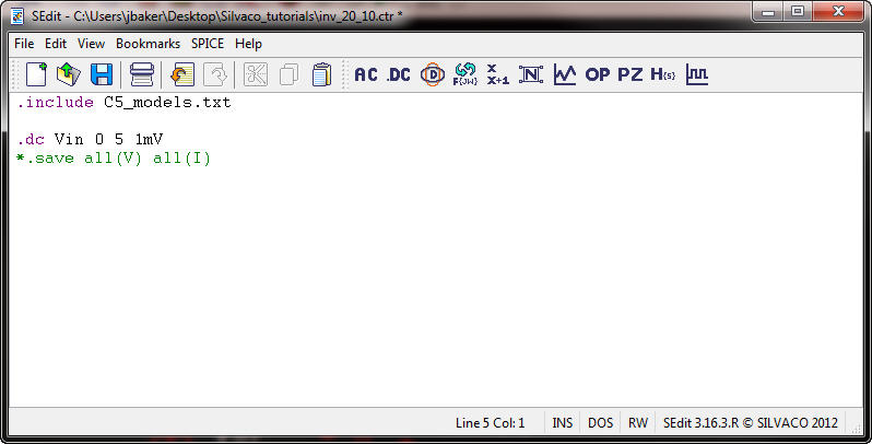
The next thing we
need to do is create a control file for simulating with SmartSpice.
We do this by
clicking on the icon seen below (do this now).
Type the following
into the control file.
The first line
specifies the SPICE models that we saved in the Silvaco_tutorial folder
on the
desktop earlier in the tutorial.
The .dc line
specifies that we are going to sweep the Vin source from 0 to 5 V in 1
mV
steps.
The last line
specifies that we save all voltages and currents in the circuit (this
line is
commented out here by adding the * to the beginning of the line)
Saving all of the
voltages and currents is fine for small simulations but isn't a good
idea in
general (the simulation results will take a lot of space and time to
manipulate).
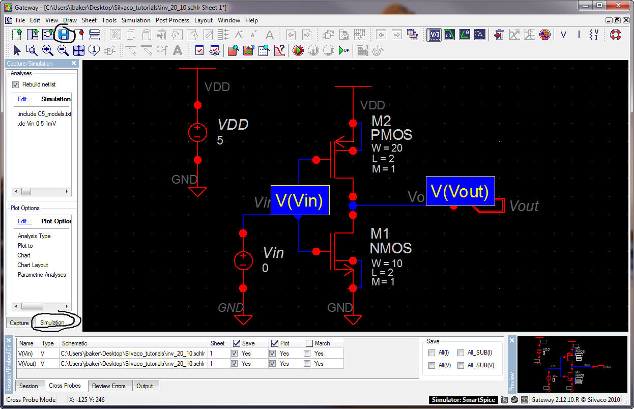
Let's specify the
signals we want to save. Before doing this save, and close, the control
file.
In the
Capture/Simulation window click on the Simulation tab as seen below.
Next click on the
Vin and Vout wires (the blue boxes will appear). These are the signals
we will
plot.
Save this
information by hitting the save icon circled below.
Click on the
Capture tab and then start the simulation by clicking on the icon seen
below.
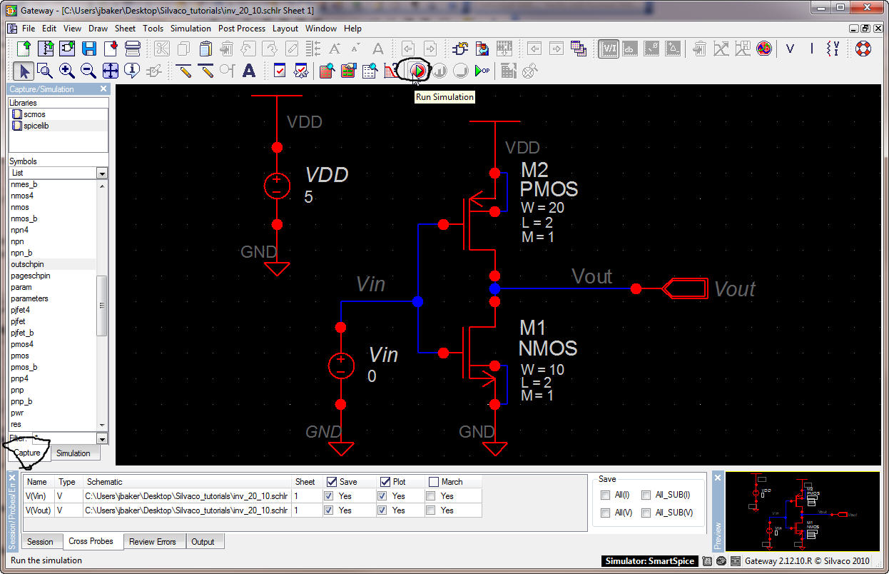
The simulation has
errors, see below.
Select the
"View Output File" icon.
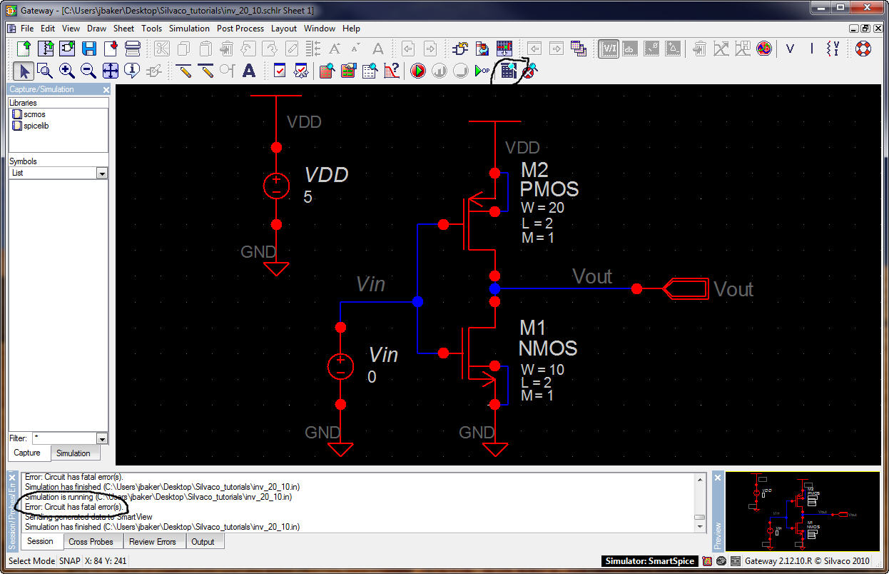
The following
window appears.
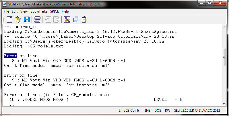
Use CTRL+F
and enter "error" to search for errors in the output file.
What we see,
below, is that SmartSpice isn't finding the models.
Verify that the
C5_models.txt
file is located in the Silvaco_tutorials folder on your desktop.
Also verify that
nothing is misspelled.
Everything looks
okay so let's open the C5_models.txt file in the Silvaco_tutorials
folder on
the desktop.
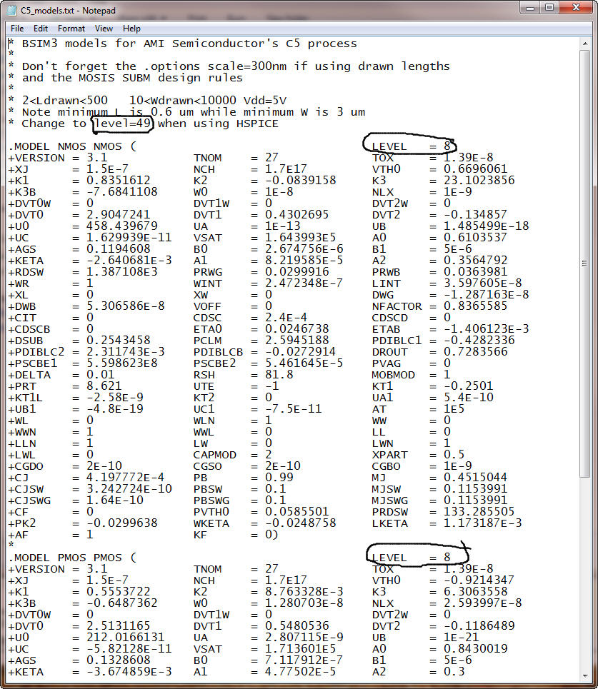
Note the comment
that for HSPICE (and SmartSpice)
we should change the level from
8 to 49 (do this and save the file).
(I've now modified
the C5_models.txt files at CMOSedu.com to indicate that both level=49
should be
used for both HSPICE and SmartSPICE).
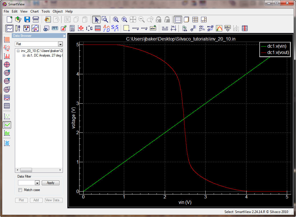
Running the
simulation again results in SmartView starting and
the waveforms we
selected being plotted, below.
Close this SmartView
window and return to Gateway.
Let's pause for a
moment and take a look at the contents of the Silvaco_tutorials folder.
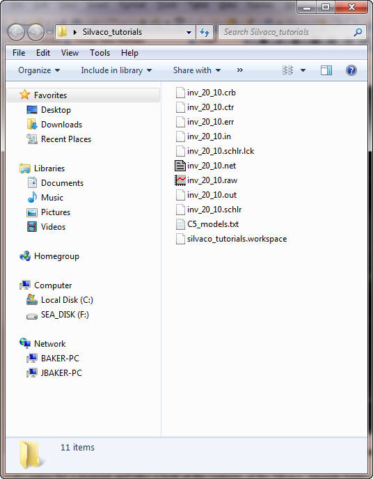
Extensions
indicate *.schlr (schematic), *.schlr.lck (a locked schematic, we are
editing
now), *.raw (SmartSpice raw simulation results used
by SmartView),
*.net (netlist),
*.err (reports
simulation errors), *.ctr (the control file), *.crb (information on
cross
probing), *.in (the SmartSpice input file, merged
*.ctr and *.net files,
for SmartSpice).
Knowing what the
files do can be useful if, for example, you don't want to re-type the
contents
of a control file.
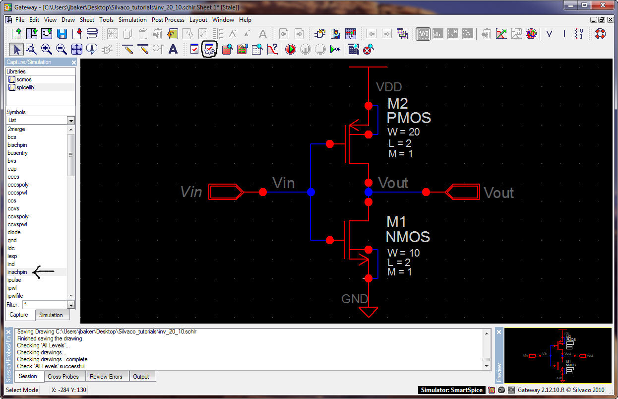
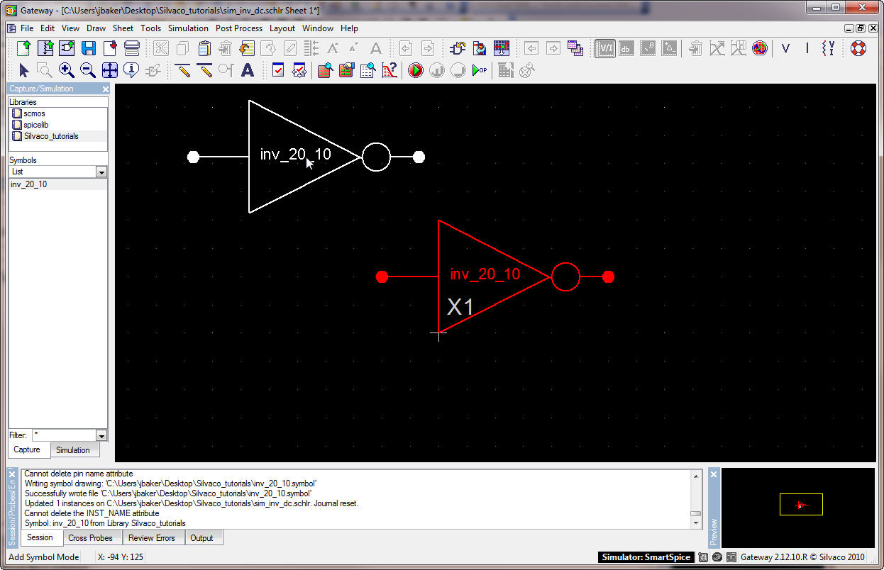
Let's make a
symbol for the inverter.
Start by deleting
the two vdc sources and adding an inschpin as seen below.
After moving the
wires and the wire names check the schematic for errors.
Then use Tools
-> Generate Symbol... to see the following
window.
Notice the shape
is set to "Not."
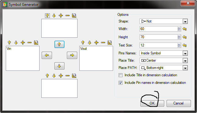
After hitting OK
we get the following Window (now there are two open windows, the
schematic and
the symbol of the inv_20_10).
To switch between
the two views (schematic and symbol) use the Window
menu selection.
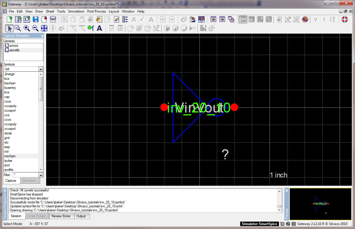
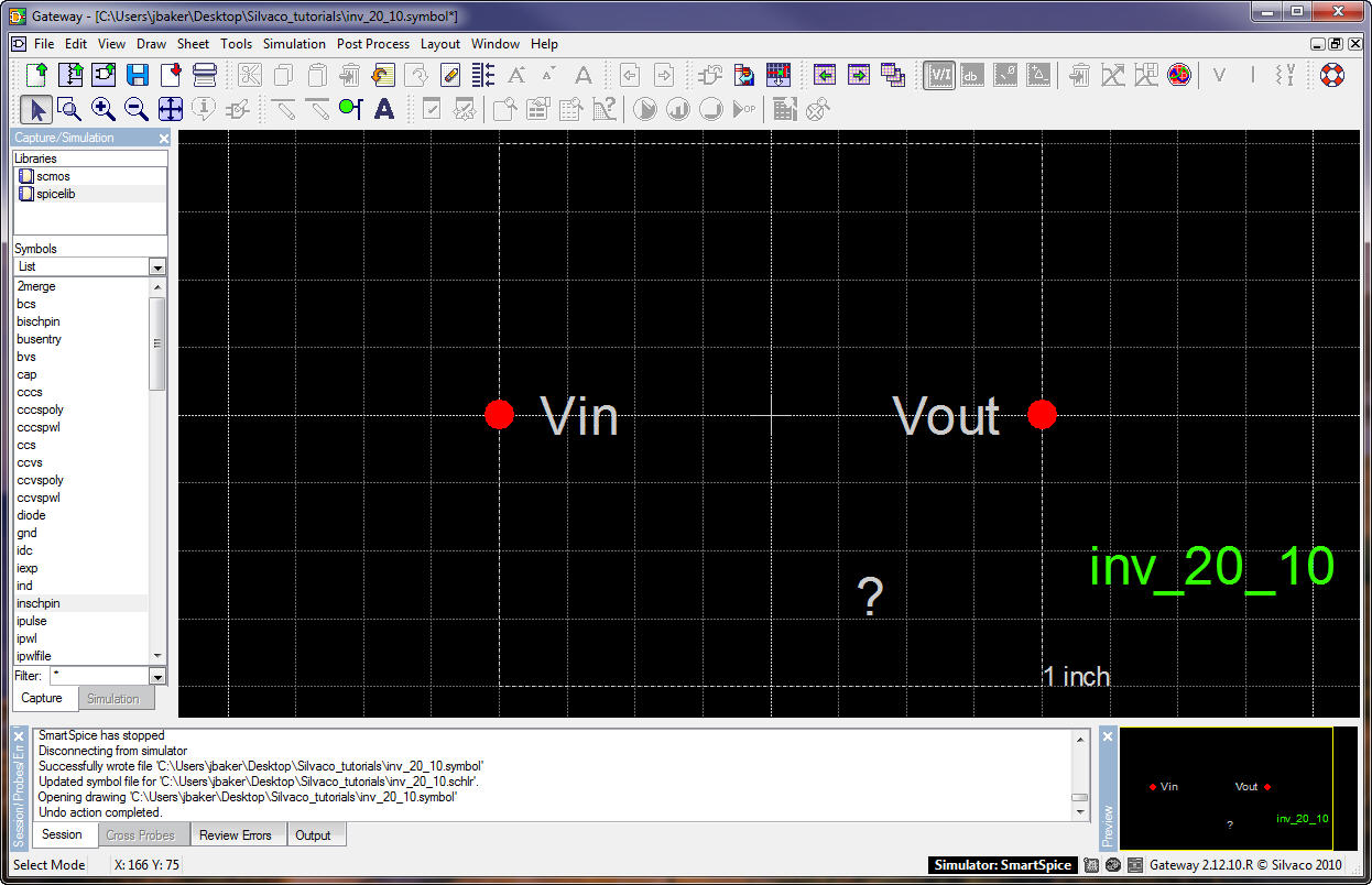
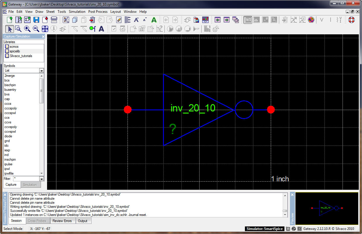
Delete all of the
blue lines, move the cell label, and pins to get the following.
Next use the Draw
-> Line (or better just press L)
to get the following.
To end drawing a
line press ESC.
To ensure that the
lines are precisely where you want them use Z (zoom
area with mouse) and
F (fit).
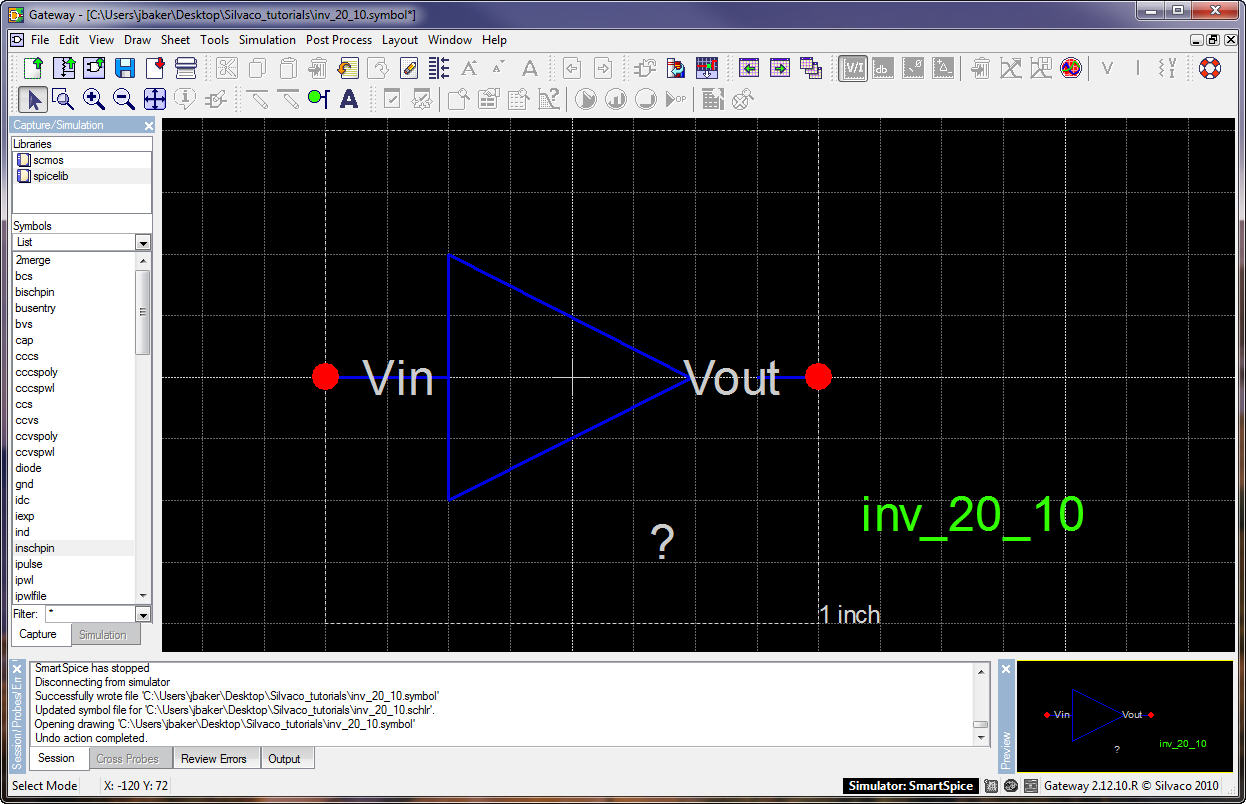
Next add a circle
(Draw -> Circle), move the ? to inside the
symbol (this is the
symbol's label, e.g., X1, when it's placed in a schematic).
Also, move, and
reduce the size of (right-click on the text and then select decrease,
or
simply press O) the symbol's name.
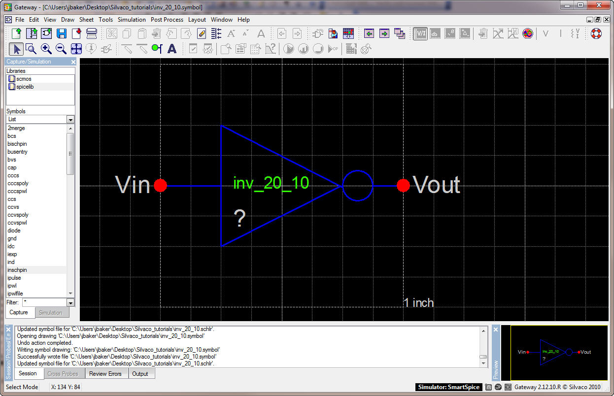
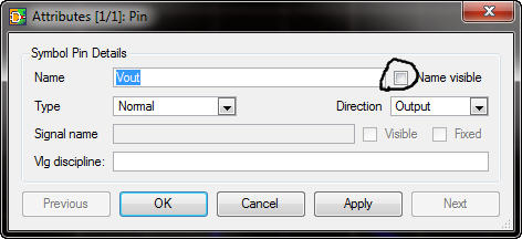
We don't need to
display the names so double click on the Vout and Vin pins and
de-select
"Name visible" as seen below.
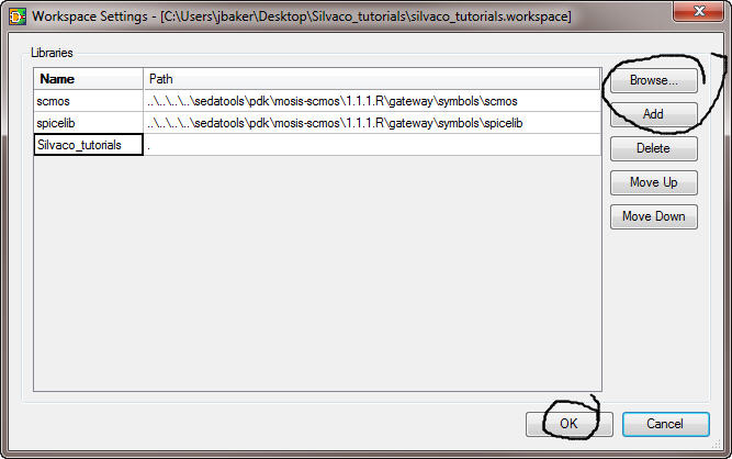
Next, we want to
be able to use this symbol in our schematics so use the menu commands File
-> Workspace Settings to open the following window.
Press the Add
button and then browse to the Silvaco_tutorials on the desktop.
Since this is the
same directory as the workspace the path is simply a period.
Change the
newlibrary Name to Silvaco_tutorials as seen below.
Press OK.
We should now see
the symbols in this Silvaco_tutorials (on the desktop) folder appear
with the
list of libraries as seen below.
Before going any
further use File -> Save Workspace to save
the workspace.
Let's do a couple
more simulation examples before quitting.
Use CTRL+N
to
create a schematic called sim_inv_dc.
Place the inverter
symbol in the schematic as seen below.
Press ESC to stop
adding the inverter symbol.
Before we go any
further select the inverter and press D (for
descend) to see what's
inside the symbol, below.
Now there are two
Windows open, the symbol and the schematic.
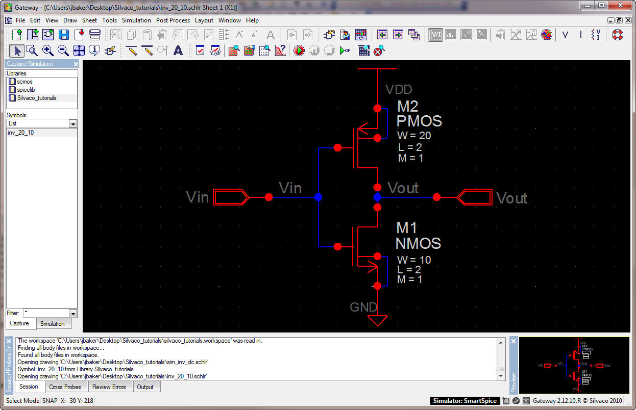
Next, with nothing
selected in the inverter symbol, press A (for
ascend) to go back to the
symbol view.
Note that both
symbol and schematic windows are still open (use the Windows menu item
to
select a specific window and C to close).
Add the following
to the sim_inv_dc schematic.
Check the
schematic and notice the warning about the dangling wire (let's ignore
it this
time).

Next select the
Simulation tab and then select the wires Vin and Vout to be plotted.
Hit Save to save
these plot settings.
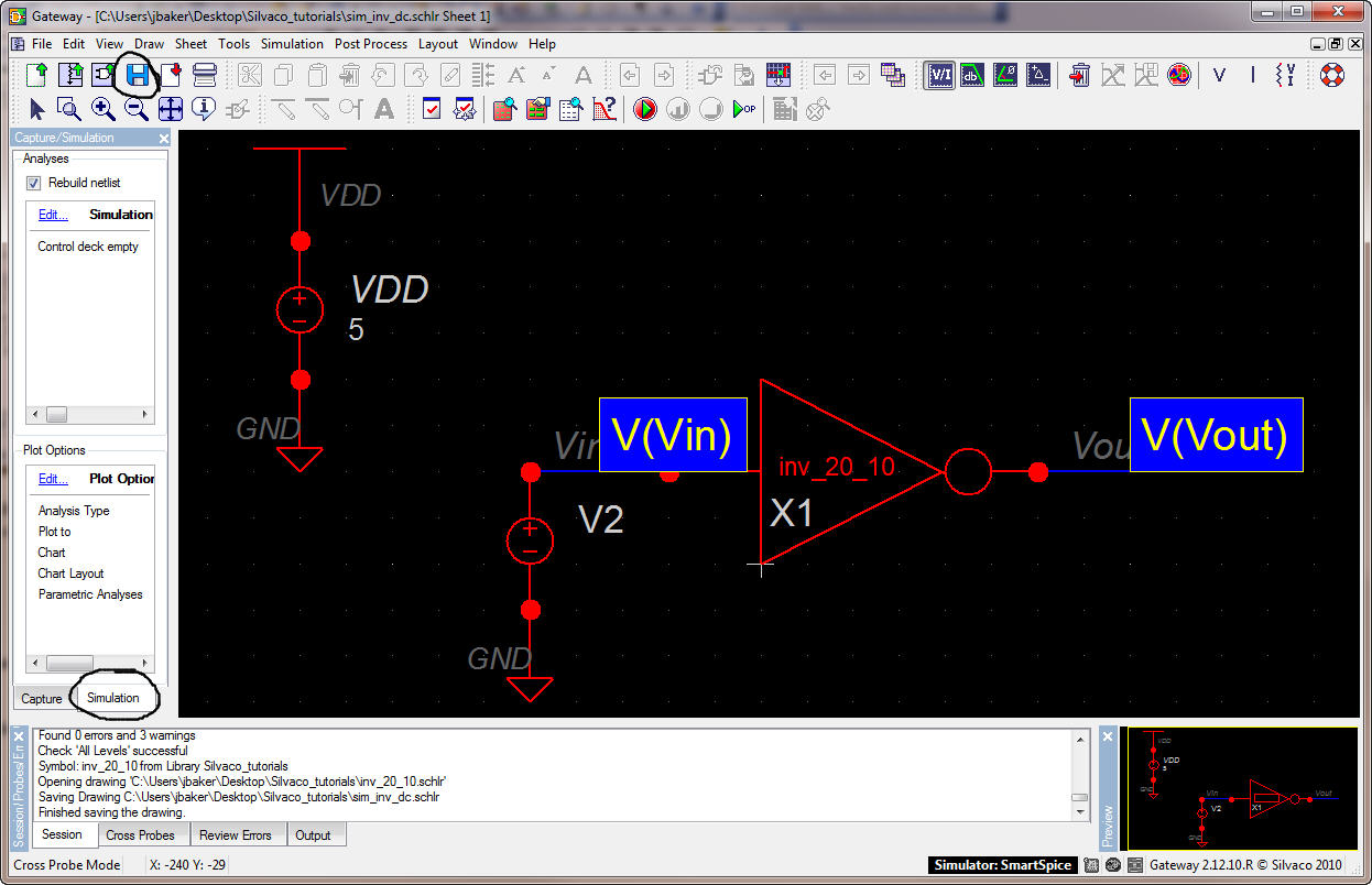
Click on the
Capture tab and then Edit the Control File and add the following.
When done save and
close the control file and then run the simulation.
We get the
following simulation output, nothing!
What's wrong?
Well, we can probably figure out the problem looking at the schematic.
However,
let's take a look at the input file.
We see that the
voltage source we are using for the inverter's input has no DC value.
Let's rename this
source and change the DC value to 0.
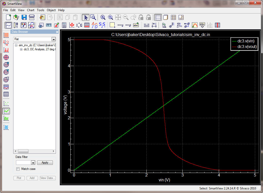
Now running the
simulation results in the following.
One last
simulation, use File - Save As to save sim_inv_dc
as sim_inv_tran (for a
transient simulation).
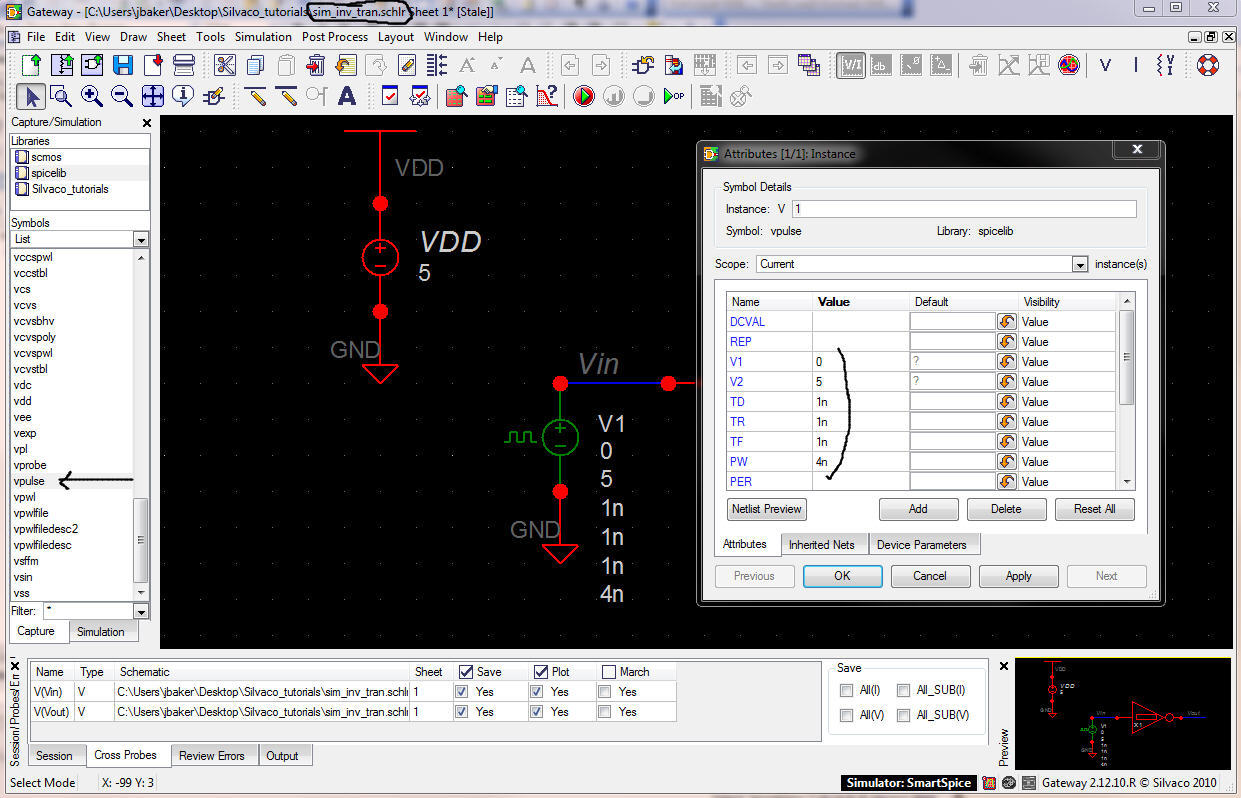
Change the input
source to a pulse and change the parameters to what is seen below.
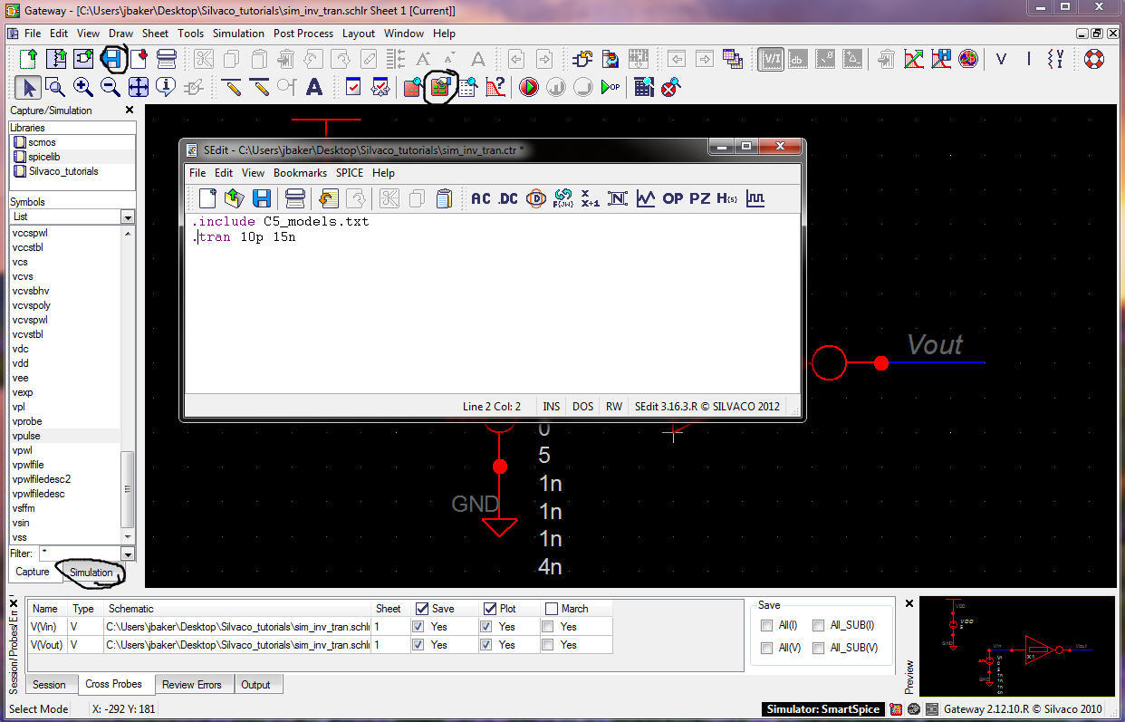
Then change the
control file to the following.
Save and close the
control file.
Click on the
Simulation tab to ensure V(Vin) and V(Vout) are still selected for
plotting
then click on the Capture tab.
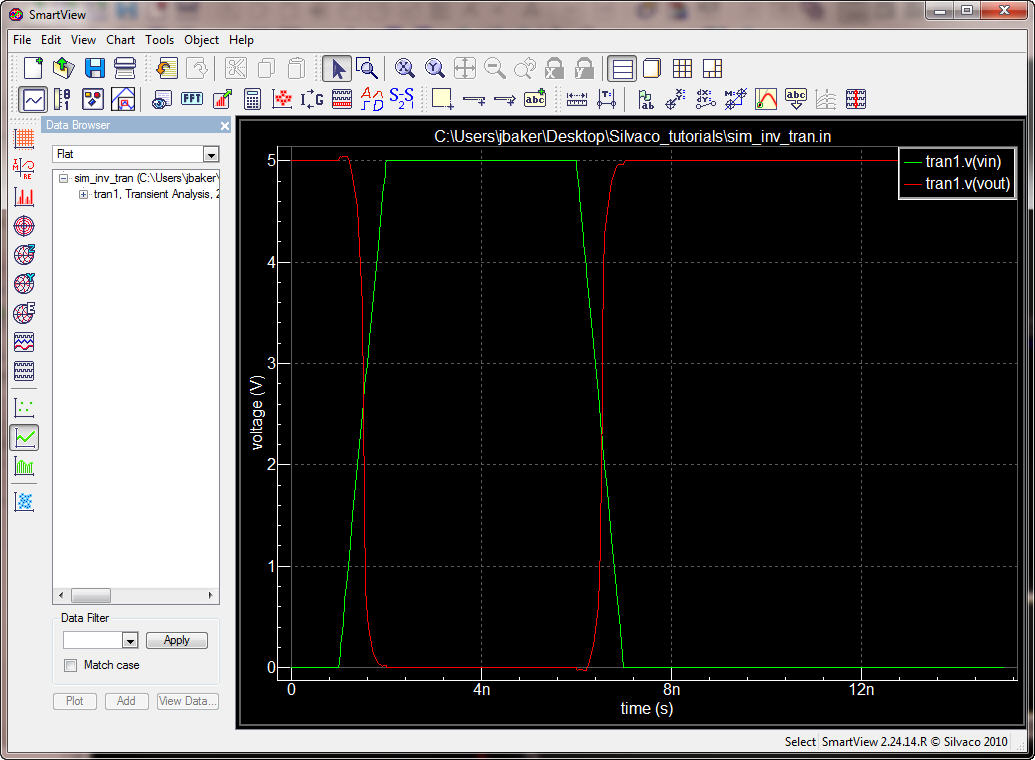
Running the
simulation results in the following.
Save and close the
sim_inv_tran schematic (and any other open schematics or symbols).
Exit Gateway.
This ends our
first tutorial.
For your reference
the final contents of the Silvaco_tutorials folder used in this
tutorial is
located in Silvaco_Tutorial_1.zip.