FTD (Fast Transient Digitizer)
R.
Jacob Baker (rjacobbaker@gmail.com)
James
Mellott (
Eric
Monahan (
Angsuman Roy (angsumanroy@gmail.com)
FTD Chip
This
test chip was fabricated using the C5 process and consists of the following
circuitry:
256 Stage FTD
w/on chip decoupling capacitor
Pad Frame/Key
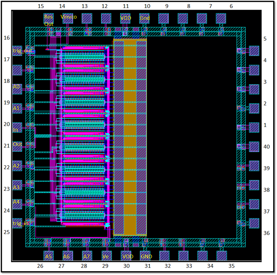
Pin Table
|
Pin # |
Name on Pad
Key |
Pin Description |
|
1 |
No Con |
n/a |
|
2 |
No Con |
n/a |
|
3 |
No Con |
n/a |
|
4 |
No Con |
n/a |
|
5 |
No Con |
n/a |
|
6 |
No Con |
n/a |
|
7 |
No Con |
n/a |
|
8 |
No Con |
n/a |
|
9 |
No Con |
n/a |
|
10 |
GND |
Ground Pad |
|
11 |
VDD |
VDD Pad |
|
12 |
No Con |
n/a |
|
13 |
No Con |
n/a |
|
14 |
Vinvco |
Bias
Generator Control Voltage |
|
15 |
Res Out |
Bias
Generator Resistor to set Current |
|
16 |
Trig_out |
Output after
256 stages of trigger input signal |
|
17 |
N Con |
n/a |
|
18 |
A0 |
Decoder 0
input |
|
19 |
A1 |
Decoder 1
input |
|
20 |
In |
Analog
signal input Pad |
|
21 |
Out |
Analog
output Pad to off chip resistor |
|
22 |
A2 |
Decoder 2
input |
|
23 |
A3 |
Decoder 3
input |
|
24 |
A4 |
Decoder 4
input |
|
25 |
Trig_in |
Trigger
input to start capturing analog input signal |
|
26 |
A5 |
Decoder 5
input |
|
27 |
A6 |
Decoder 6
input |
|
28 |
A7 |
Decoder 7
input |
|
29 |
Ve |
Enable input
for decoder |
|
30 |
VDD |
VDD Pad |
|
31 |
GND |
Ground Pad |
|
32 |
No Con |
n/a |
|
33 |
No Con |
n/a |
|
34 |
No Con |
n/a |
|
35 |
No Con |
n/a |
|
36 |
No Con |
n/a |
|
37 |
No Con |
n/a |
|
38 |
No Con |
n/a |
|
39 |
No Con |
n/a |
|
40 |
No Con |
n/a |
Pin Table
FTD
|
Component |
Trigger In |
Trigger Out |
Analog In |
Analog Out |
Ground |
|
FTD |
Pin 25 |
Pin 16 |
Pin 20 |
Pin 21 |
10, 31 |
FTD Flow Chart
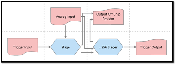
Fast Transient Digitizer
The
Fast Transient Digitizer captures a fast signal in
adjustable time intervals which can be read out at a slower speed to analyze
the data. The adjustable time intervals between each capture varies from
0.929 ns to 6 ns per stage. The read out process
is done using a series of 4x16 decoders which can access any stage to determine
the “strength” of the analog signal at that time which can be determined by
knowing when the Trigger Input goes low and the time interval between the
stages.
This
work is the continuation of the Transient Digitizer
Integrated Circuit Design with improvements in layout and circuit design.
Single Stage Layout
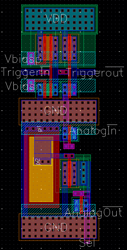
This
new layout structure per stage is laid out according to the signal flow which
results in better performance over earlier designs, also the Analog Input and
Output signal lines were separated to reduce induced noise.
Bias Generation
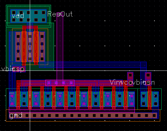
The Bias Generation circuit allows us to adjust the time interval
between each stage. Each stage utilizes two current starved MOSFET’s
which are controlled from the bias generation circuit above.