EE
421L Digital Integrated Circuit Design - Lab 7
Using
buses and arrays in the design of word inverters, muxes, and high-speed
adders
Pre-lab
work
- Back-up all of your
work from the lab and the course.
- Go through Tutorial 5 seen here.
- Read through the entire lab before starting it.
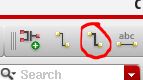
Wide wires (buses) are added using the bindkey shift+W or the menu button seen circled below.
Arrayed symbols (by changing the symbol's name) are used to make schematics concise and easier to use.
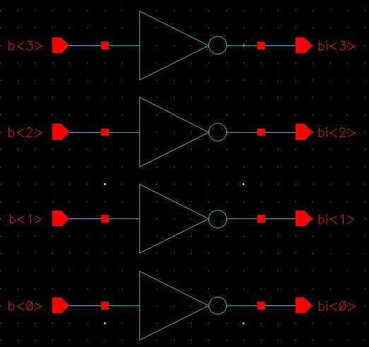
Examine the circuit used for inverting a 4-bit word seen below.
The inverter uses 6u/0.6u NMOS and PMOS devices.
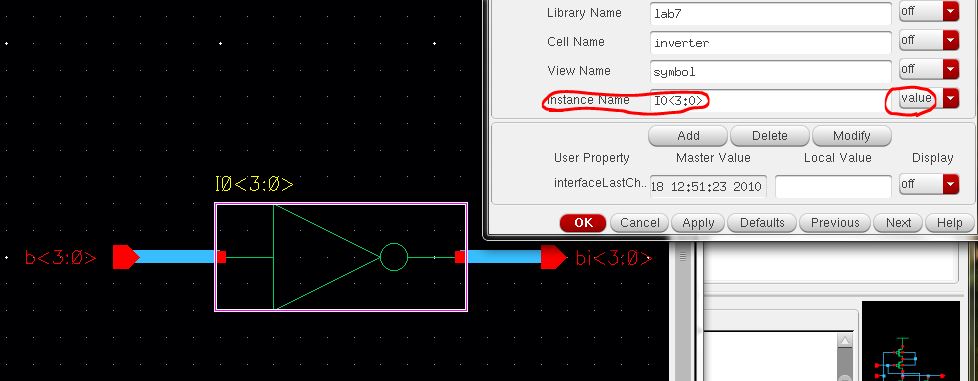
We can make an equivalent, more concise, schematic by instantiating an
inverter
and naming the inverter using an arrayed name (I0<3:0> see image below).
Connect a wide-wire (bus) as seen below and connect it to input and output pins.
Name the pins as seen below.
This schematic equivalent to the one seen above but obviously more concise.
For your lab report please use cell names that indicate the current semester and your initials.
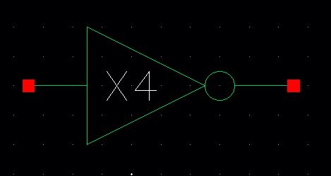
Create a symbol for the schematic, something like the following.
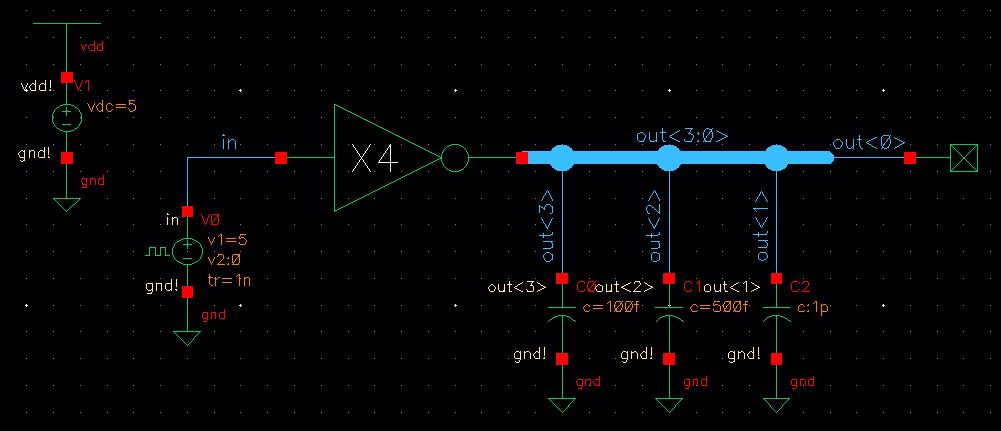
Using this symbol create a simulation schematic like the one seen
below.
All four inverters' inputs are tied together to an input pulse source.
The out<0> is not connected to a load while out<3> is connected to a 100fF load.
The out<1> is connected to a 1 pF load while out<2> is connected to a 500 fF load.
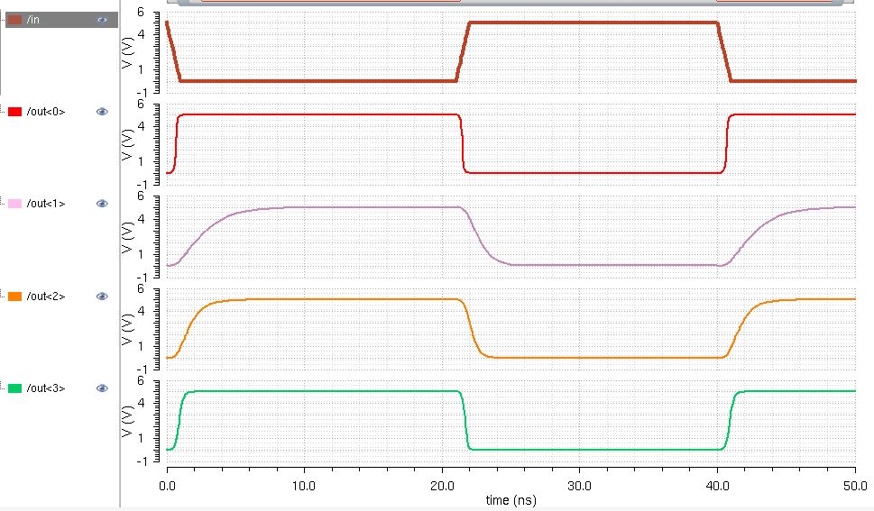
Simulating this schematic results in the following.
Show, in your lab report, how a capacitive load influences the delay and rise/fall times.
Create schematics and symbols for an 8-bit input/output array of: NAND,
NOR, AND,
inverter, and OR gates.
Provide a few simulation examples using these gates.
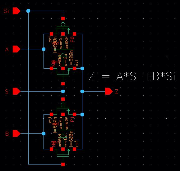
Next examine the following schematic.
This is the schematic of a 2-to-1 DEMUX/MUX (and the symbol).
Simulate the operation of this circuit using Spectre and explain how it
works.
Make sure to show, using simulations, how the circuit can be used for both multiplexing and de-multiplexing.
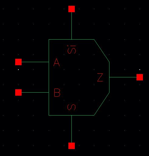
Create an 8-bit wide word 2-to-1 DEMUX/MUX schematic and symbol.
Include an inverter in your design so the cell only needs one select
input, S
(the complement, Si, is generated using an inverter).
Use simulations to verify the operation of
your
design.
Finally, draft the schematic of the full-adder seen in Fig. 12.20 using
6u/0.6u
devices (both PMOS and NMOS).
Create an adder symbol for this circuit (see the symbol used in lab6).
Use this symbol to draft an 8-bit adder schematic and symbol.
For how to label the bus so the carry out of one full-adder goes to the
carry
in of another full-adder review the ring oscillator schematic discussed
in Cadence
Tutorial 5.
Simulate the operation of your 8-bit adder.
Lay out this 8-bit adder cell (*note* that this is the only layout required in this
lab).
Show that your layout DRCs and LVSs correctly.
This ends lab 7. We've covered all of the basic building
blocks used in an
ALU.
The cells used to generate the images used on this webpage are found in lab7.zip.
Ensure that your html lab report includes your name and email address
at the
beginning of the report (the top of the webpage).
When finished backup your work (webpages
and design
directory).