EE 421L Digital Integrated Circuit Design -
Lab 2
Design
of a 10-bit digital-to-analog converter (DAC)
Pre-lab work
- Back-up all of your work from the lab and the course.
- Read through this entire lab write-up before doing the pre-lab
- Download lab2.zip
to your desktop.
- This archive
contains a simulation example using an ideal 10-bit
Analog-to-Digital Converter (ADC) and Digital-to-Analog Converter
(DAC).
- Upload this zip file to the design
directory on the server that you are running Cadence from, e.g.,
Tutorial_1, CMOSedu, etc.
- Note that it's
assumed you are using the NCSU Cadence Design Kits.
- Unzip this directory and add, to your
cds.lib in the design directory, the following statement (assuming the
design directory is CMOSedu):
- DEFINE lab2 $HOME/CMOSedu/lab2
- Start Cadence from the design
directory.
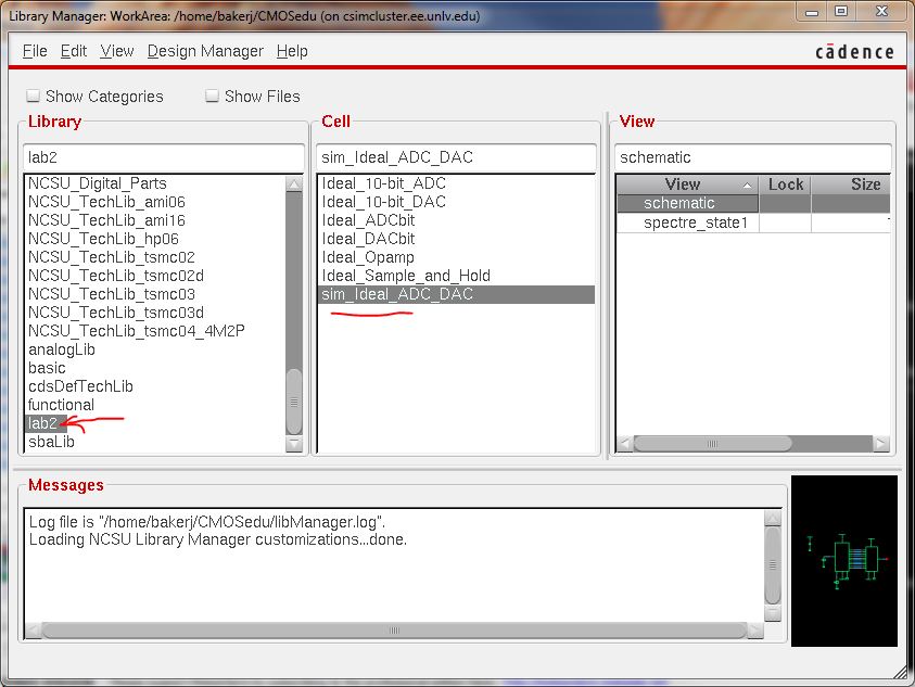
- Use the Library
Manager and navigate to the lab2 Library as seen below.
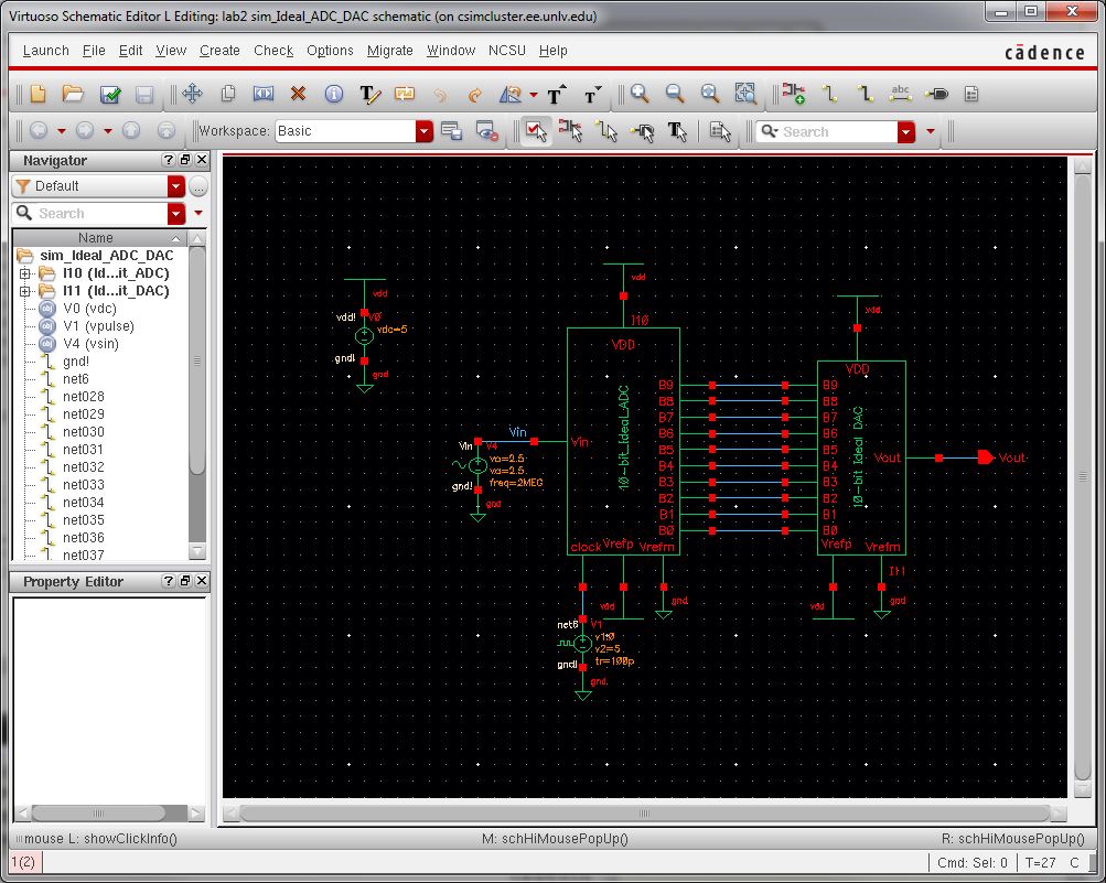
- Open the schematic view of the cell sim_Ideal_ADC_DAC.
- This cell contains
the ideal 10-bit ADC and DAC as seen below in the second image.
- Run the simulation (Launch the ADE, Session -> Load State -> Cellview -> OK, press the green start button) to get the following.
- Make sure you understand how to change the background color, line thickness, and type of line (e.g. solid, dashed, etc.)
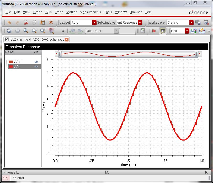
- Prior to coming to lab make sure you
understand how the input voltage, Vin, is related to B[9:0] and Vout (the quiz may ask a question about this).
- In your lab report: 1) provide
narrative of the steps seen above, 2) provide, and discuss, simulation
results different from the above to illustrate your understanding of the
ADC and DAC, 3) explain how you determine the least significant bit (LSB,
the minumum voltage change on the ADC's input to
see a change in the digital code B[9:0]) of the
converter. Use simulations to support your understanding.
- Backup your webpages and design diretory.
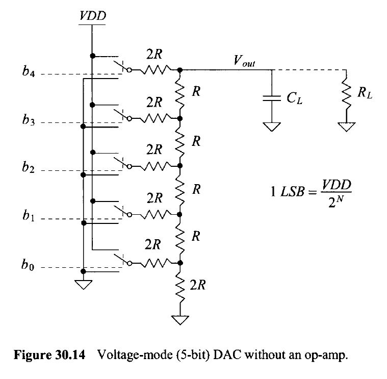
In this
lab we'll use n-well resistors to implement a 10-bit DAC.
Our design is based upon the topology seen in Fig. 30.14, below, in the
CMOS book.
The controlling input bits seen below come from the ADC, in other words
the inputs to the DAC are the left side of the 2R resistors.
Your lab report should document the following:
- The design of a 10-bit DAC using an
n-well R of 10k
- The 2R resistor
should be implement with two separate 10k resistors in series
- After you've
designed and drafted your schematic check and save it
- How to determine the output resistance
of the DAC (answer: R) by combining resistors in parallel and
series
- Delay, driving a load
- Ground all DAC
inputs except B9. Connect B9 to a pulse source (0 to VDD) and show, and
predict using 0.7RC, the delay the DAC has driving a 10 pF load
- Verify the
simulation results match your hand calculations
- How
to create a symbol view for your design with the exact same footprint
as the Ideal_10-bit_DAC symbol view (hint: use Copy before you
start drafting your design, e.g. Copy the cell Ideal_10-bit_DAC to
Mydesign_10-bit_DAC and then simply edit the schematic view!)
- See Tutorial 1 for additional help
- Note that your design won't use VDD, Verfp, or Vrefm so you can delete those pins on your design's DAC symbol view
- Simulations to verify your design
functions correctly.
- Copy the schematic
cell view sim_Ideal_ADC_DAC to a cell sim2_Ideal_ADC_DAC and replace the ideal
DAC with the one you just designed
- Use the
sim2_Ideal_ADC_DAC to illustrate that your design works as
expected.
- Show what happens
if the DAC you designed drives a load (both R, C, and R/C)
- Explain what
happens if the DAC drives a 10k load?
- In a real circuit the switches seen above (the outputs of the ADC) are
implemented with transistors (MOSFETs).
- Discuss what happens if the resistance of the switches isn't small compared to R.
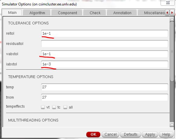
- If you have simulation convergence problems you can force the simulation to converge by going to, in the ADE, Simulation -> Options -> Analog
- Set the values as seen below
- relative tolerance, reltol, of 10% (= 1e-1)
- voltage absolute tolerance, vabstol, of 100 mV (= 1e-1)
- current absolute tolerance, iabstol, of 1 mA (= 1e-3)
- The accuracy of the simulation will, obviously, be degraded
Ensure
that your html lab report includes your name and email address at the beginning
of the report (the top of the webpage).
When finished backup your work (webpages and design directory).