EE
421L Digital Integrated Circuit Design - Lab 7
Using
buses and arrays in the design of word inverters, muxes, and high-speed
adders
Pre-lab
work
- Back-up all of your
work from the lab and the course.
- Go through Tutorial 5 seen here.
- Read through the entire lab before starting it.
Buses
and arrayed icons (by changing
the icon's name) are used to make schematics concise and
easier to use.
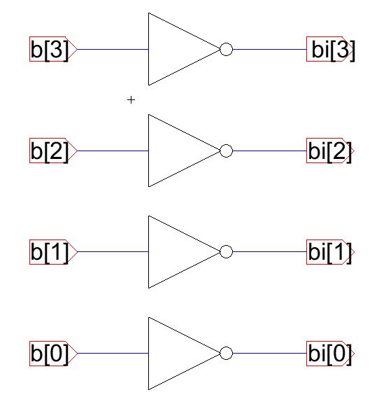
Examine the circuit used for inverting a 4-bit word seen below.
The inverter uses a 20/2 PMOS and a 10/2 NMOS as seen in lab7.jelib.
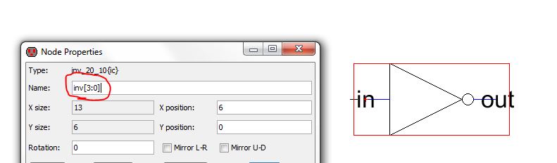
We can make an equivalent, more concise, schematic by instantiating an
inverter
and naming the inverter using an arrayed name.
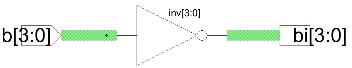
The result, for the example seen below, is 4 inverters represented by a
single
inverter icon.
Again,
for your lab report, please use cell names that indicate
the current semester and your initials.
Adding a bus (the green line) to off-page connections makes
this schematic
equivalent to the one seen above but obviously more concise.
Note
that inv[3]'s input is b[3] and its output is bi[3]
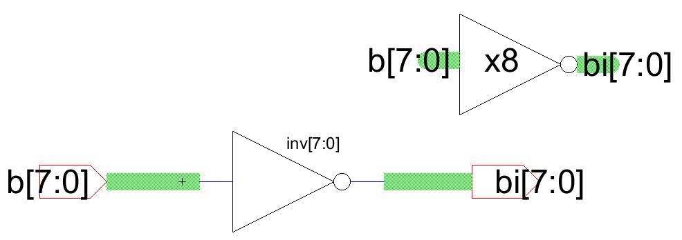
Okay, make a schematic for a building block useful in, for
example, an ALU
for inverting an 8-bit word (needed for subtraction).
An example is seen below noting the icon view looks like an inverter
with a
"x8" to indicate 8 inverters.
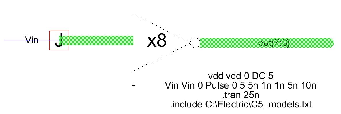
Using this icon create a simulation schematic like the one seen
below.
The Wire_con icon (the
box with a J in its center) is
used to connect the input bus lines together and to a wire called Vin.
This junction connection is used when changing bus sizes.
The output bus is labeled out[7:0].
A label isn't required and if one isn't provided Electric will name the
bus.
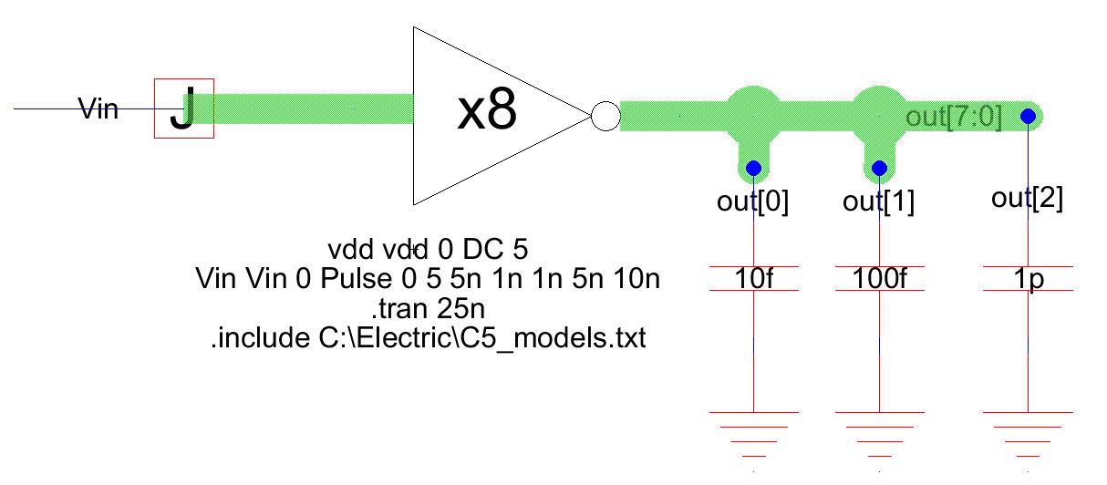
Let's do one more simulation before moving on.
Let's put various capacitive loads on the output of 3 of the 8
inverters as
seen below.
Wires can be connected directly to a "bus pin" as long as the wire is
named (so Electric knows which signal on the bus to connect the wire
to).
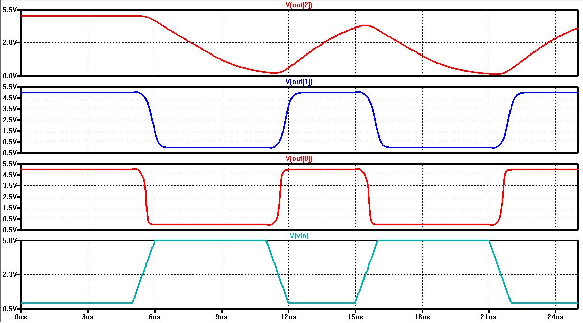
Below are the simulation results.
Obviously the output of the inverter can't drive a 1 pF load very
quickly.
Create schematics and icons for an 8-bit input/output array of: NAND,
NOR, AND,
and OR gates.
Provide a few simulation examples using these gates (use all four of
them in a
single schematic with the x8 inverter to show operation using an 8-bit
input/output bus).
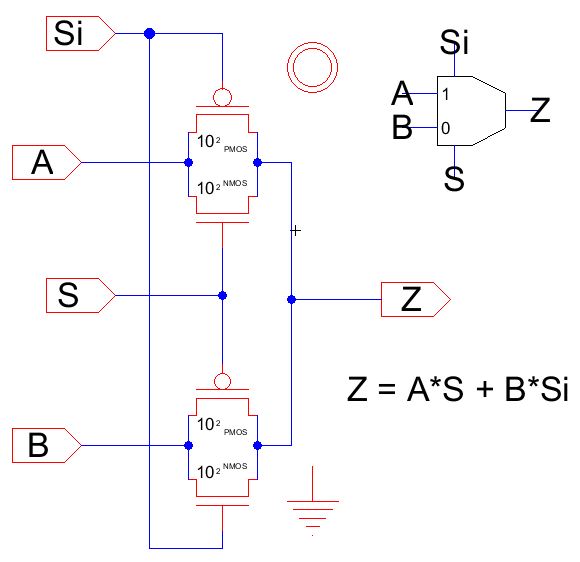
Next examine the following schematic.
This is the schematic of a 2-to-1 DEMUX (and the icon).
Si is the logical complement to S (adding the "i"
indicates "invert")
Simulate the operation of this circuit using SPICE and explain how it
works.
Can this circuit be used with Z as an input and A/B as outputs (can it
be used
as a MUX)?
Verify your response using simulations.
Create an 8-bit wide word 2-to-1 DEMUX/MUX schematic and icon.
Include an inverter in your design so the cell only needs one select
input, S
(the complement, Si, is generated using the inverter).
Use simulations (both IRSIM and LTspice) to verify the operation of
your
design.
Finally, draft the schematic of the full-adder seen in Fig. 12.20 using
6/2
devices (both PMOS and NMOS).
Create an adder icon for this circuit (see icon used in lab6).
Use this icon to draft an 8-bit adder schematic and icon.
For how to label the bus so the carry out of one full-adder goes to the
carry
in of another full-adder review the ring oscillator schematic discussed
in
Tutorial 5.
Simulate the operation of your adder using IRSIM.
Lay out the 8-bit adder (note this is the only layout required in this
lab).
Show that your layout NCCs, DRCs, and Well checks without errors
(provide the jelib in
your lab directory).
This ends lab 7. We've covered all of the basic building
blocks used in an
ALU.
Ensure that your html lab report includes your name and email address
at the
beginning of the report (the top of the webpage).
When finished backup your work (webpages
and design
directory).