Digital IC Design - Lab 4 - EE421L
Author: Brian Wolak,
Email: wolak@unlv.nevada.edu
September 15, 2021
Lab Description
This
lab will focus on the IV characteristics, layout, and simulation of
PMOS and NMOS devices in the ON Semiconductor Cadence C5 Process.
Pre-Laboratory Procedure
- Before starting this lab, all previous work was backed up using .zip files and my personal Google Drive.
- The lab was read in its entirety to be prepared for instruction after covering all material found in Tutorial 2
Laboratory Objectives
1.) Generate the 4 schematics and simulations below
- 6u/600n NMOS simulating ID v. VDS varying VGS from 0-5V in 1V steps while VDS varies from 0-2V in 1mV steps
- 6u/600n NMOS simulating ID v. VGS for VDS = 100mV where VGS varies from 0-2V in 1mV steps
- 12u/600n PMOS simulating ID v. VSD for VSG varying 0-5V in 1V steps with VSD varying 0-5V in 1mV steps
- 12u/600n PMOS simulating ID v. VSG for VSD = 100mV varying VSG 0-2V in 1mV steps
2.) Lay out a 6u/600n NMOS connecting all 4 terminals to probe pads adjacent to the MOSFET device
- Show DRC confirmation and corresponding schematic with proof of LVS
3.) Lay out a 12u/600n PMOS connecting all 4 terminals to probe pads adjacent to the MOSFET device
- Show DRC confirmation and corresponding schematic with proof of LVS
Laboratory ProcedureThis
lab begins with creating the testing schematics with probe pads for
each NMOS and PMOS device along with a symbol for each. Below you can
see the results of each PMOS and NMOS device circuit and thier
respective symbol created using Cadence Design software.

Figure 1: NMOS schematic with pads

Figure 2: NMOS Symbol
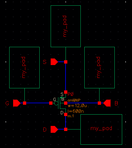
Figure 3: PMOS schematic with pads
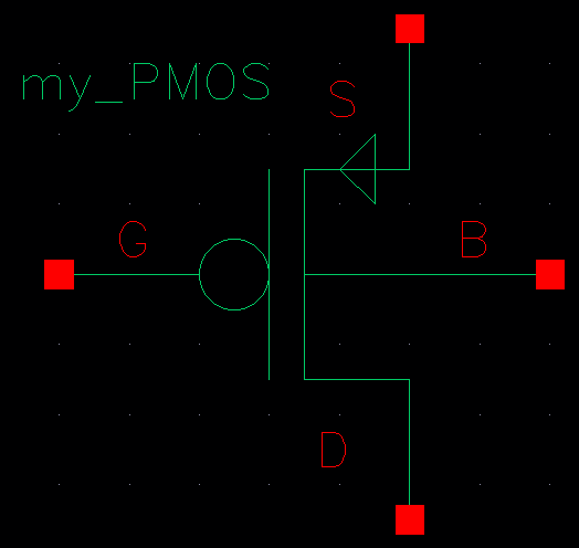
Figure 4: PMOS Symbol
Simulations
A series of simulations will now be performed to obtain the appropriate IV cruves for each device.
NMOS Device - ID v. VDS
- VGS will vary from 0-5V in 1V steps while VDS sweeps 0-2V in 1mV steps


Figures 5-6: NMOS Simulation circuit and results simulating ID v. VDS
NMOS Device - ID v. VGS
- VDS = 100mV while VGS is swept from 0-2V in 1mV steps

Figures 6-7: NMOS Simulation circuit and results simulating ID v. VGS
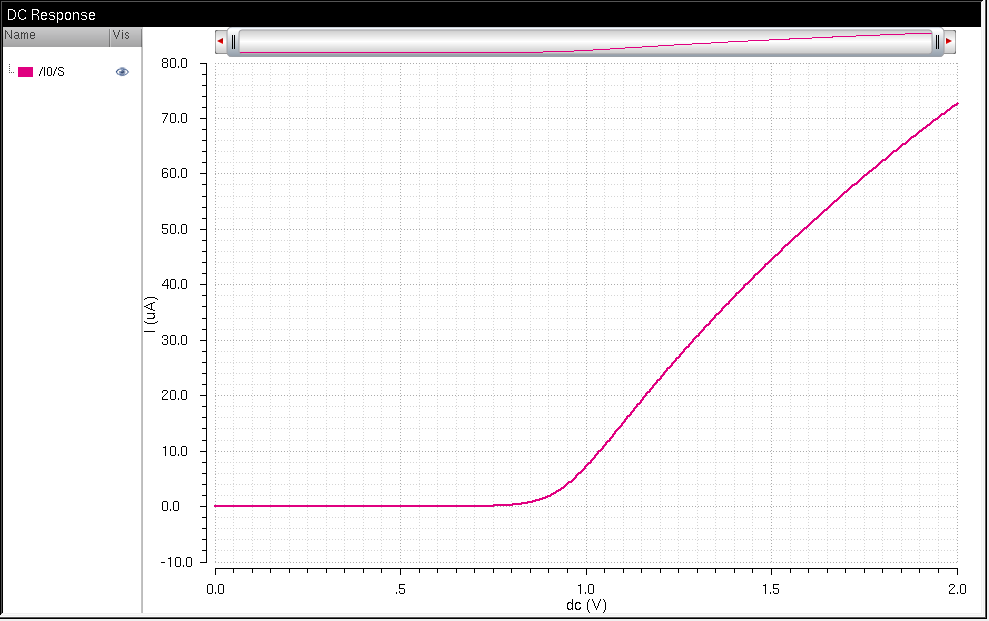
PMOS Device - ID v. VSD
- VSG is swept from 0-5V in 1V steps with VSD varying 0-5V in 1mV steps


Figures 8-9: PMOS simulation circuit and results simulating ID v. VSD
PMOS Device - ID v. VSG
- VSD = 100mV varying VSG 0-2V in 1mV steps

Figures 10-11: PMOS simulation circuit and results simulating ID v. VSG
PMOS 12.0um / 600nm Layout
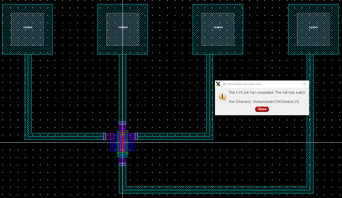
Figure 12: PMOS layout showing probe pads and LVS confirmation

Figure 13: PMOS DRC Confirmation
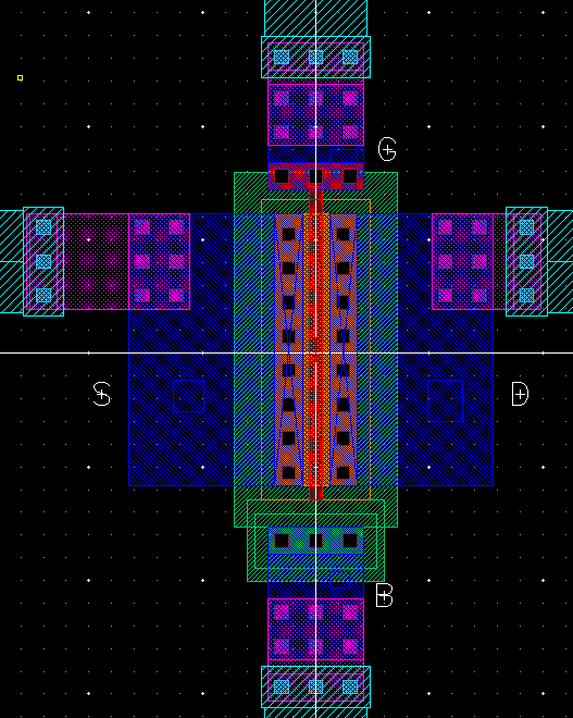
Figure 14: Zoomed in view of PMOS device layout
NMOS 6.0um / 600nm Layout

Figure 15: NMOS layout showing probe pads and LVS confirmation

Figure 16: NMOS DRC Confirmation

Figure 17: Zoomed view of NMOS device layout
Backups
As with all prevous labs, work was periodically backed up using .zip files and my personal Google Drive


Return to EE421 Labs
Return to EE421 Lab Fall 2021
