Lab Project - Register File - EE 421L Fall 2021
Authored
by: Anthony Torres
Email: torrea20@unlv.nevada.edu
Due Date: November 24, 2021
Project Description
The
project is to design a register file that uses an 8-bit word and has 32
words. In order to acces the 32 8-bit words the register file
uses a 5-bit address. Overall the inputs for the register file
include vdd/gnd, 8-IO lines for reading and writing, a control signal
and read/write input. Along with the schematic, symbol and
simulation for the register file each component followed by register
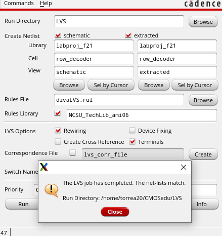
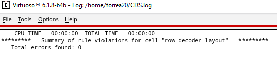
file has its own layout and extracted view that will be DRC and LVS
checked to ensure there are no errors within the design and that the
net-list match.
Main Components
In order to design the register file the project was divided into the main componets which are the - SRAM, 8-bit Word, 32 8-bit words, 5 input NAND gate, Inverter, Row Decoder and Register File.
Each component were done seperatly so that the layout of each
component would have no erros for a DRC check and have the net-list
match for a LVS check.
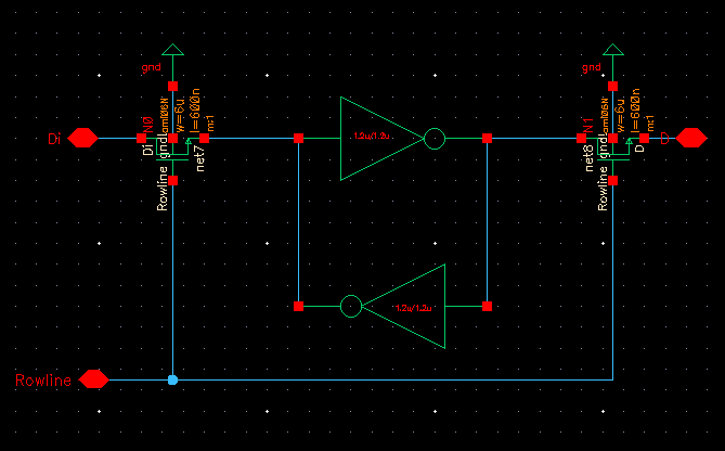
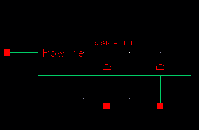
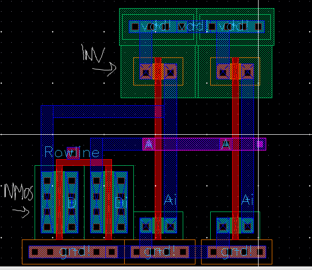
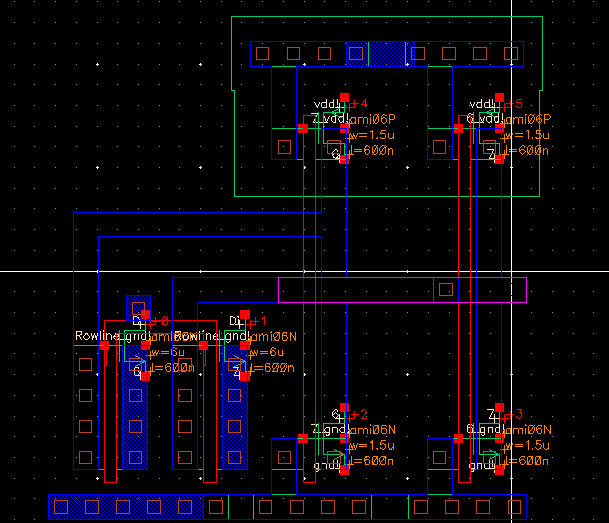
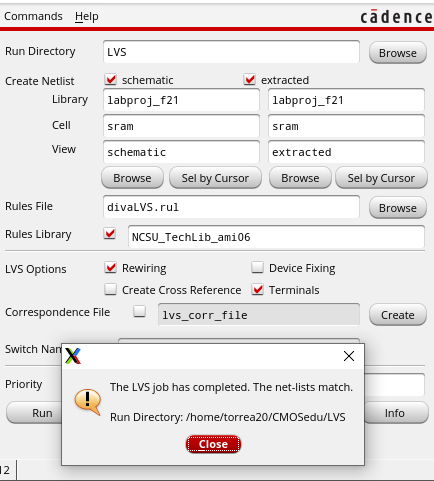
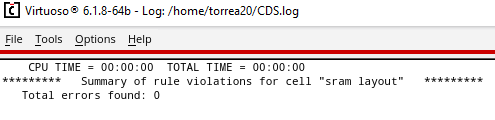
SRAM
The
Static Random Access Memory(SRAM) cell is 1-bit of data it includes 3
inputs D,Di and Rowline. The purpose of D,Di is to send a signal
that will change the value inverters because they are stronger
transistors compared to the inverters which are set to minimum size
(1.5u/1.5u) so that they can be changed quickly. When rowline is
high the values can be changed(write) and when rowline is low the
values are set(read). Shown below are screenshots of the
schematic, symbol, layout and extracted views. Included with the
layout is the DRC and LVS check to ensure that there are no errors and
the netlist match.
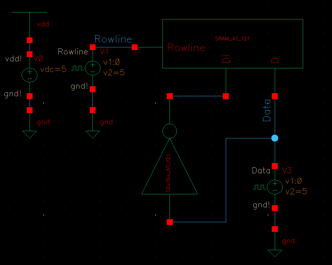
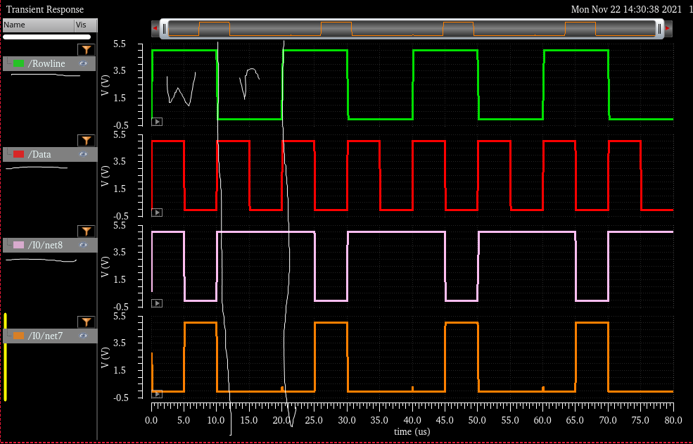
The following screenshots show the
simulation setup/results showing that the SRAM cell is reading and
writing the data as the rowline changes.
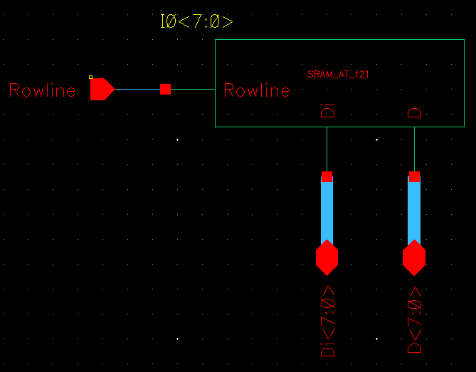
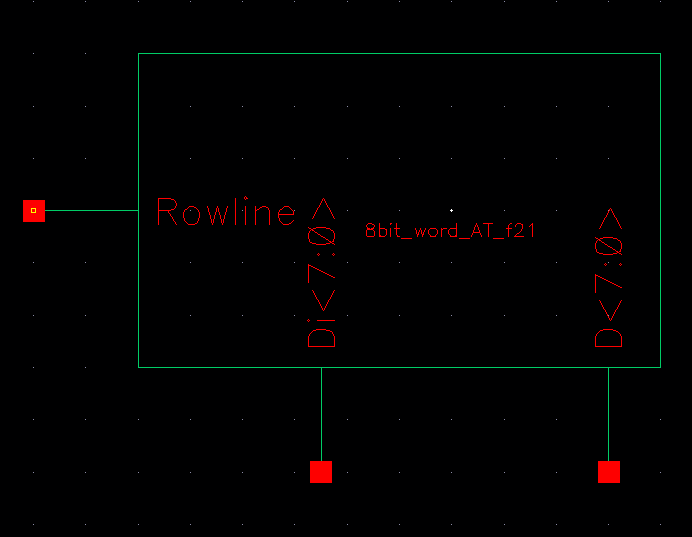
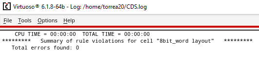
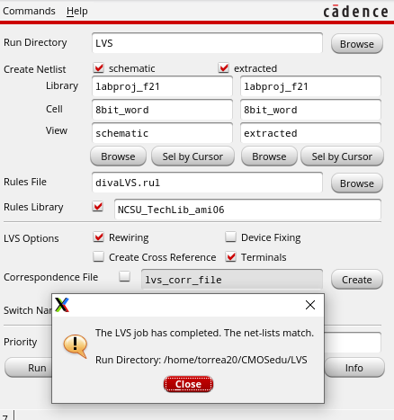
8-bit Word
The
8-bit word consist of creating an arry of the SRAM cell that would have
all the rowlines connected and having each bit have its own D,Di inputs
that range from D<7:0>, Di<7:0>. The operation of
this cell works just like the SRAM with the only change being that each
bit will have a different value depending on the D,Di input. Shown below are screenshots
of the schematic, symbol, layout and extracted views. Included with
the layout is the DRC and LVS check to ensure that there are no errors
and the netlist match.
The
following screenshots
show the simulation setup/results showing that the 8-bit word cell
reads and writes correctly depending on if the inputs are set high or
low.
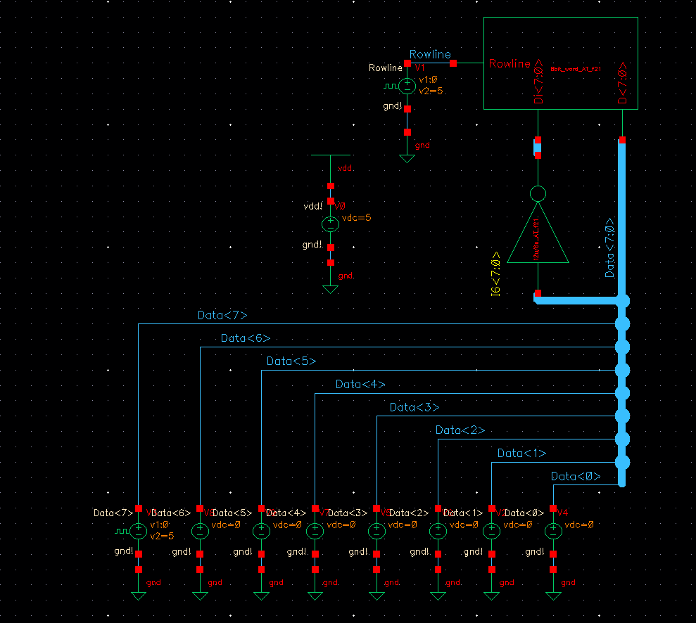
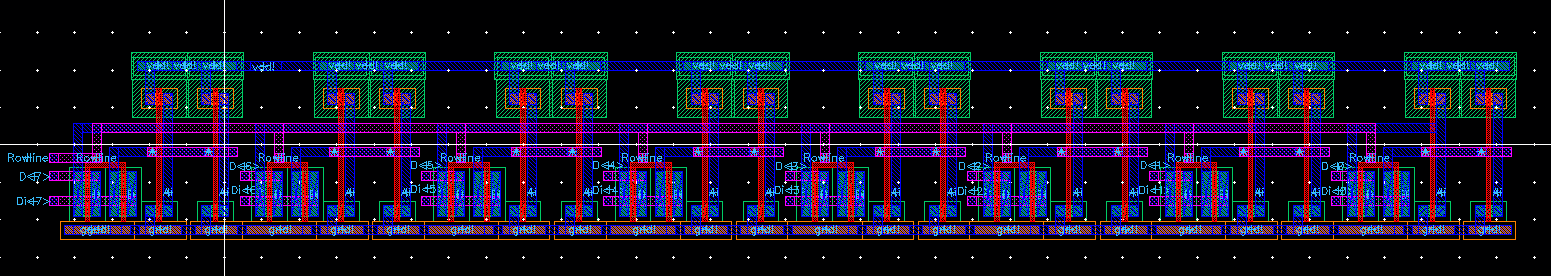
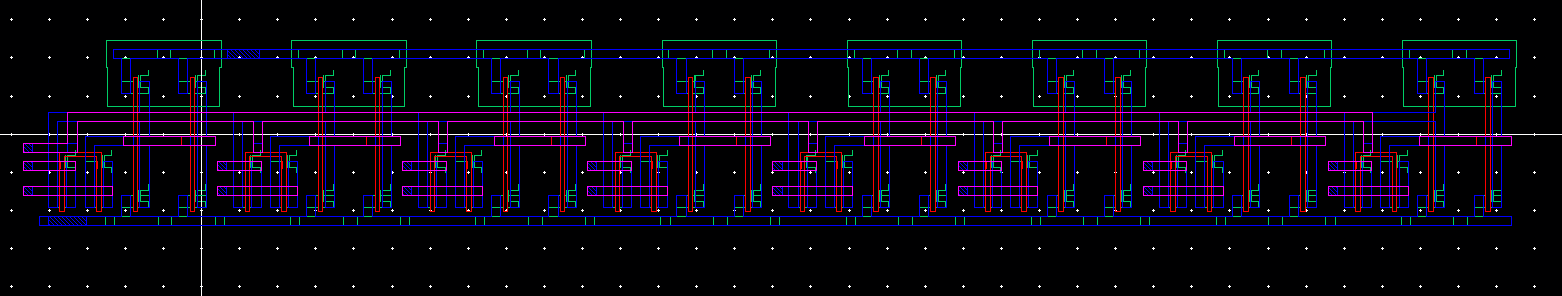
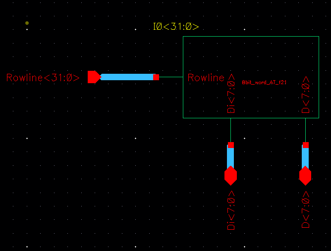
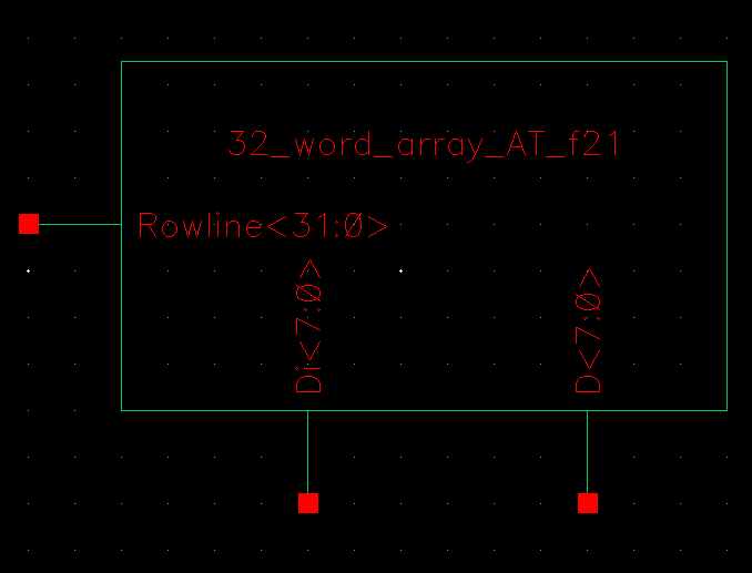
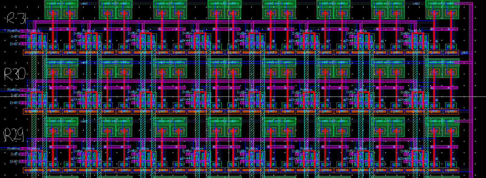
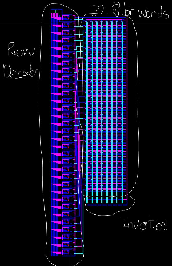
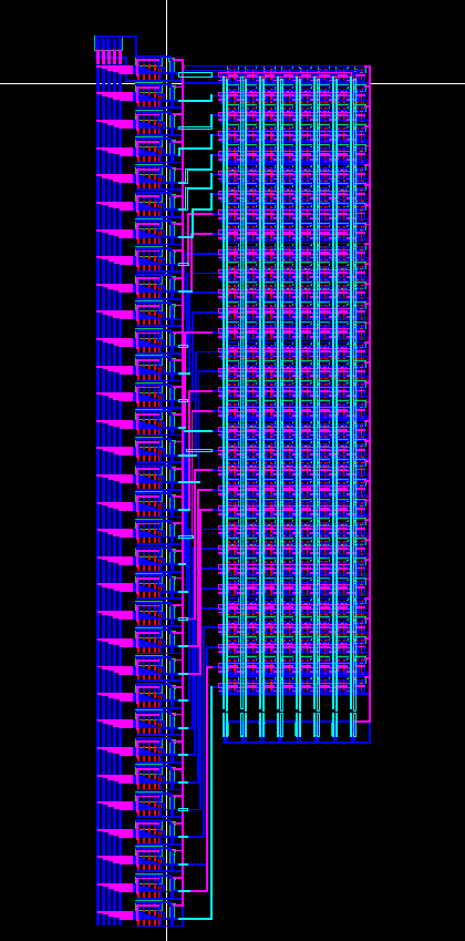
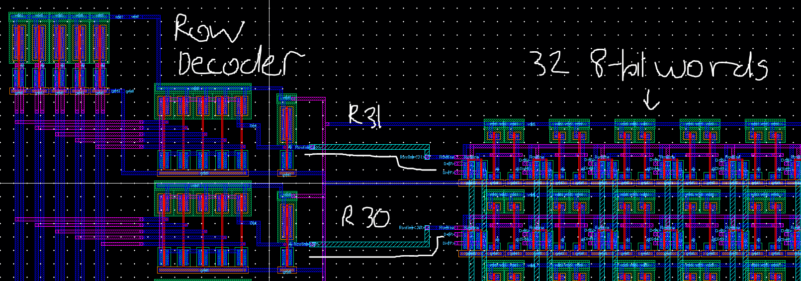
32 8-bit words
The
32 8-bit words consist of creating an array of the 8-bit word that has
32 different rowlines shown as Rowline<31:0> this is so that each
rowline will have its own value determine by the D,Di inputs that range
8-bits shown as D<7:0>,Di<7:0>. The operation of the
cell works just like the 8-bit word with the only difference being each
row has its own 8-bit word.
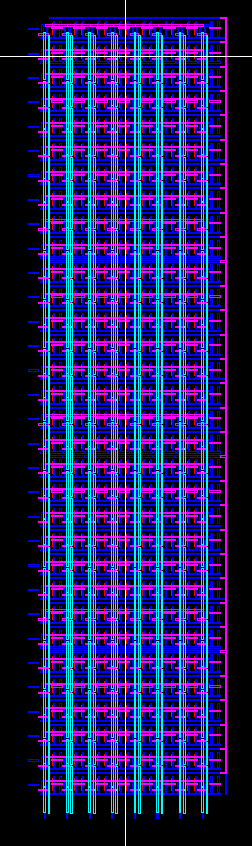
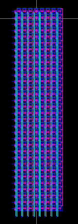
Shown below are screenshots
of the schematic, symbol, layout and extracted views. For the
layout a zoomed in screenshot is also included to show how each row is
connected. Included with
the layout is the DRC and LVS check to ensure that there are no errors
and the netlist match.
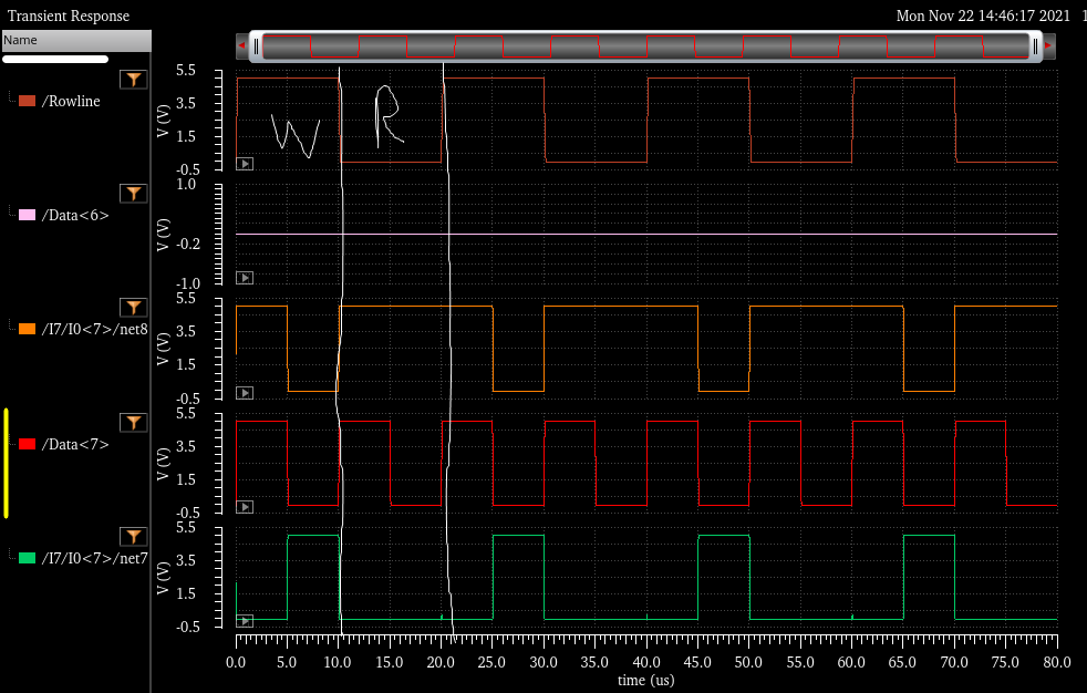
The
following screenshots
show the simulation setup/results showing that the 32 8-bit words cell
reads and writes depending on the input value assigning it to that
specific row.
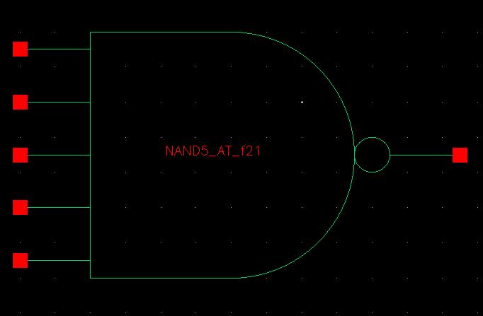
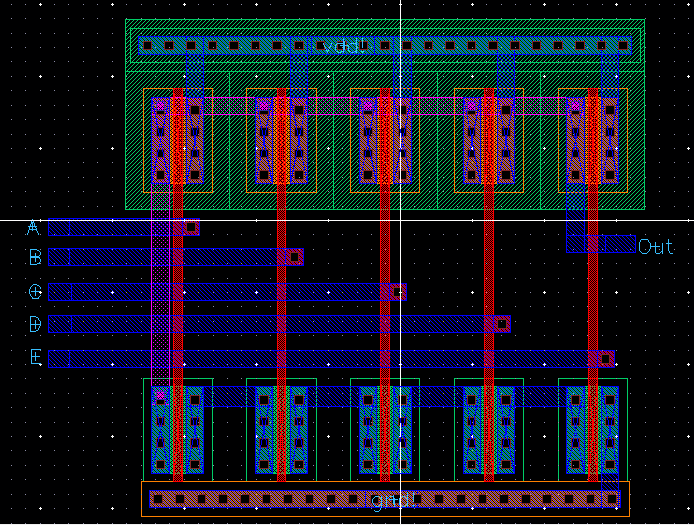
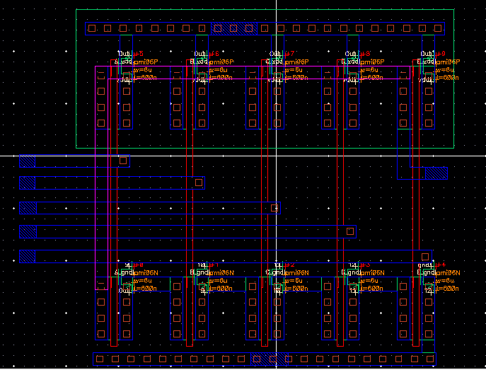
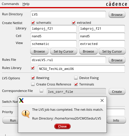
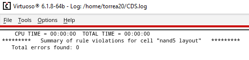
NAND gate
The nand gate has 5 inputs that will be the 5 bit address that is set to each rowline. Shown below are screenshots
of the schematic, symbol, layout and extracted views. Included with
the layout is the DRC and LVS check to ensure that there are no errors
and the netlist match.
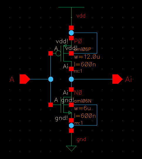
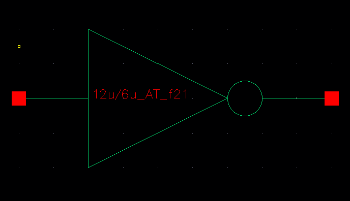
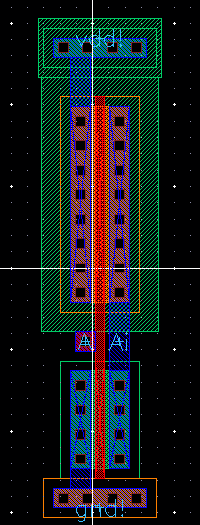
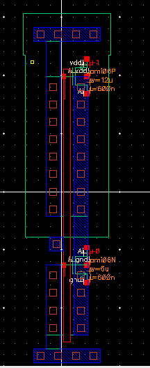
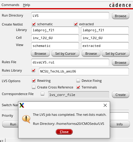
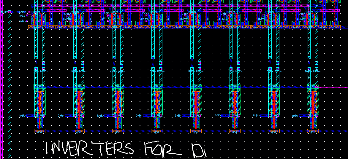
Inverter
The 12u/6u will follow each NAND gate along with each D input to set the Di input. Shown below are screenshots
of the schematic, symbol, layout and extracted views. Included with
the layout is the DRC and LVS check to ensure that there are no errors
and the netlist match.
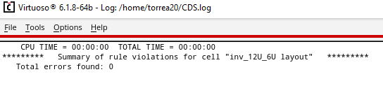
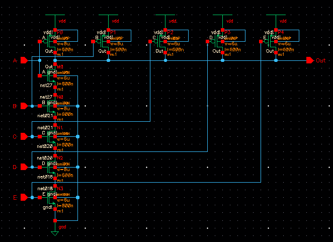
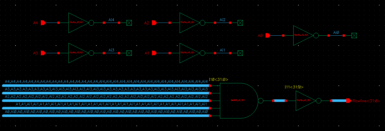
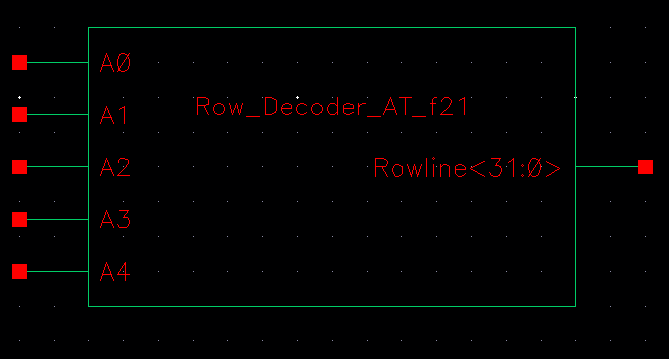
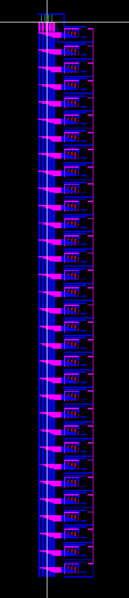
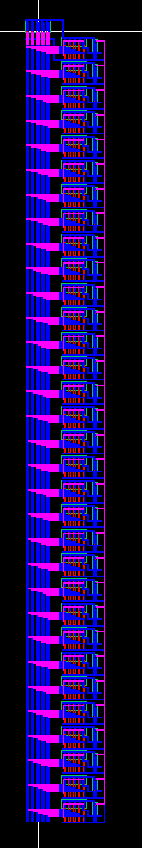
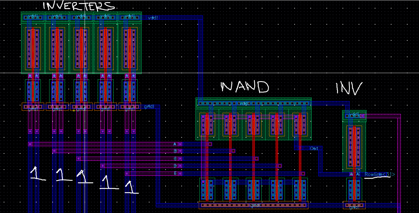
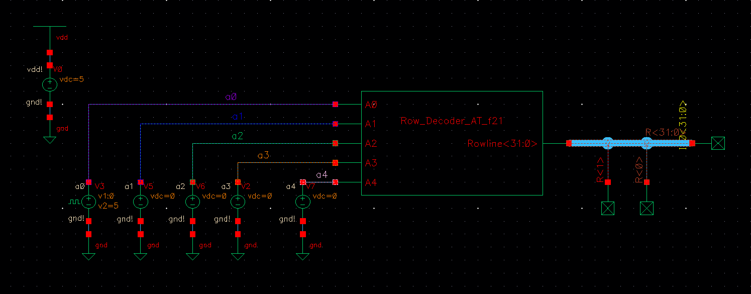
Row Decoder
The
row decoder consist of 5 inputs that will be set to an inverter in
order to get its complement. Those inputs will be feed into a
NAND gate followed by and inverter to determine which row it will be
calling in the 32 8-bit words. Shown below are screenshots
of the truth table, schematic, symbol, layout and extracted views. For the layout a
zoomed in screenshot is also included to show how each nand and inverter is
connected to the 5 inputs. Included with
the layout is the DRC and LVS check to ensure that there are no errors
and the netlist match.
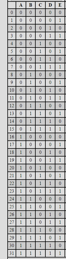
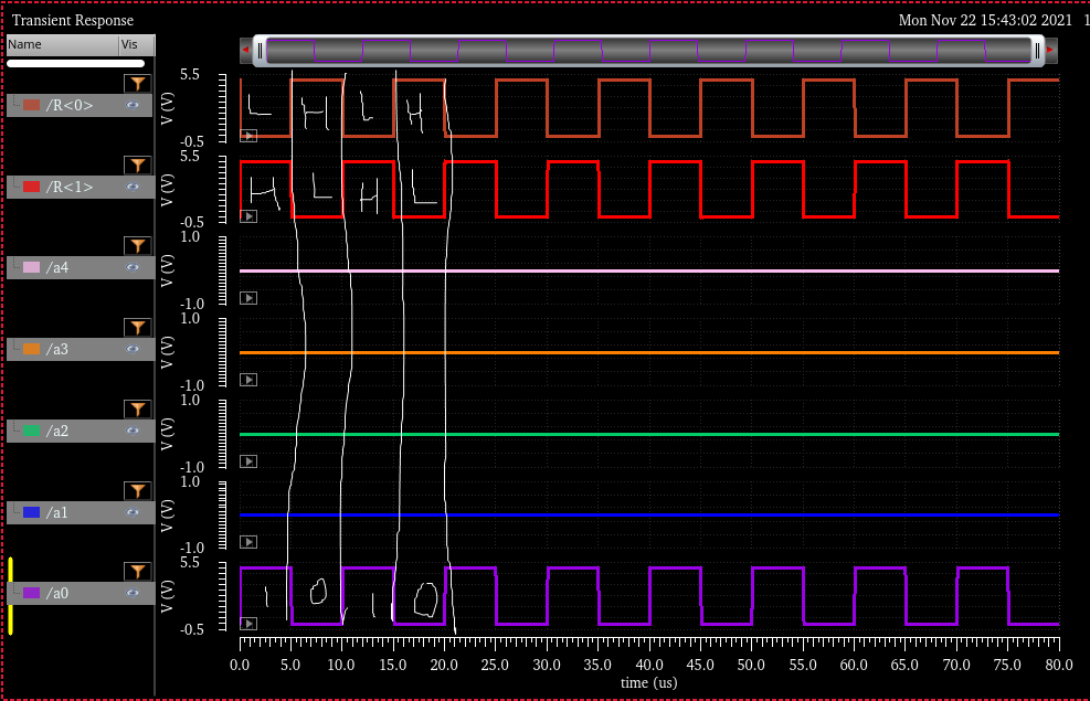
The
following screenshots
show the simulation setup/results showing the Row Decoder and how it
follows the truth table. In this case all values are set to 00000
with only the last bit being pulsed from 0 to VDD changing the values to 00000 and 00001. This
shows that when the first case is true row 0 is high and when the
second case is true row 1 is high.
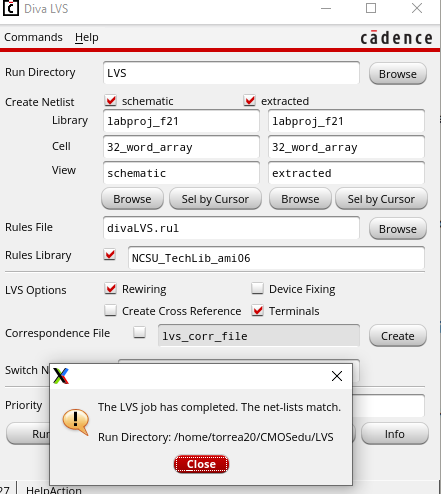
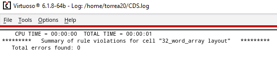
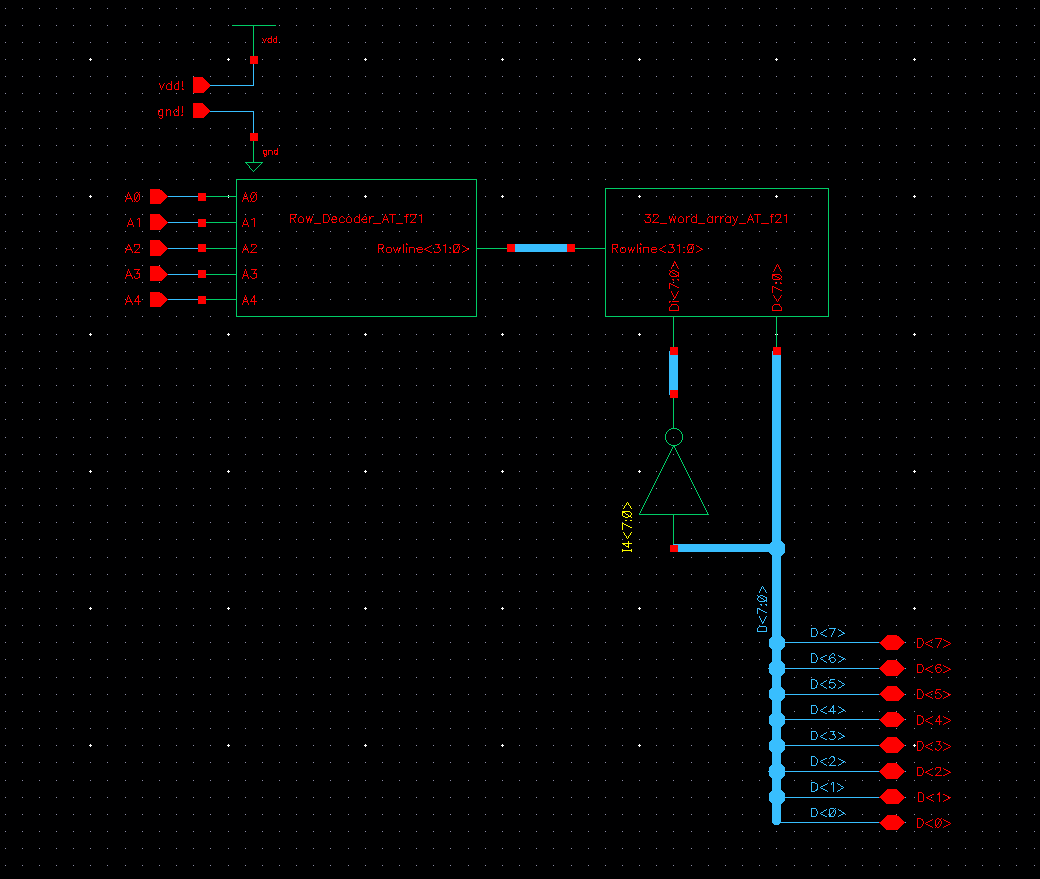
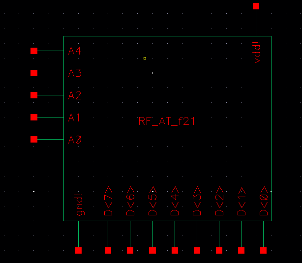
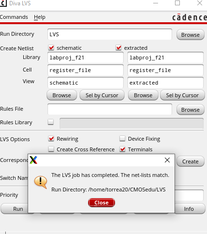
Register File
The
register file consist of connecting the row decoder to the 32 8
bit-word. The inputs for the register file will include the 5
inputs of the row decoder, vdd/gnd and the Data I/O pins of the 32 8
bit-word. Shown
below are screenshots
of the schematic, symbol, layout and extracted views. For the
layout a
zoomed in screenshot is also included to show how the rowline pins are
connected to one another as well as the inverter that will create a
complement for the Data IO pins. Included with
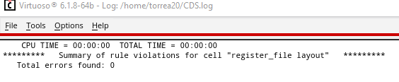
the layout is the DRC and LVS check to ensure that there are no errors
and the netlist match.
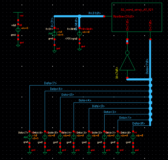
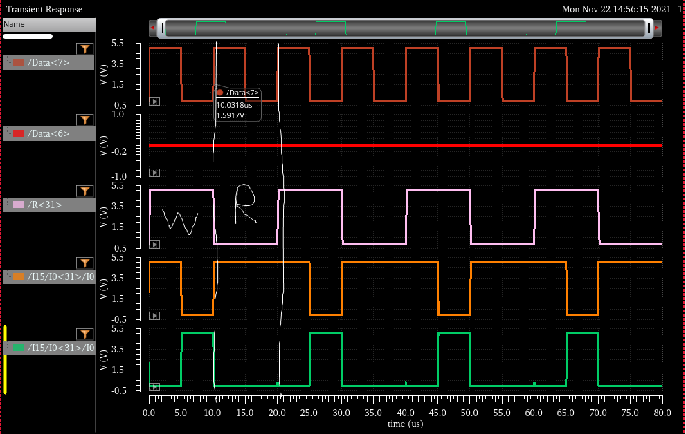
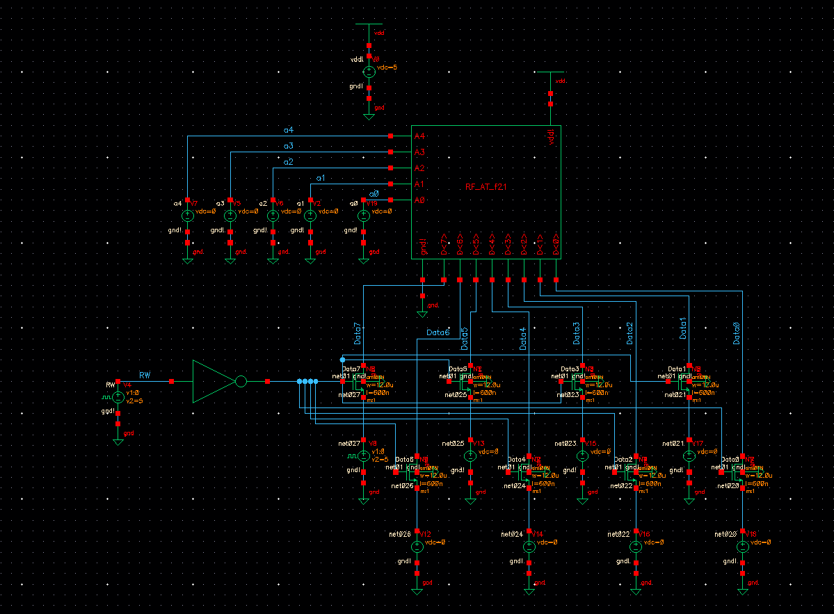
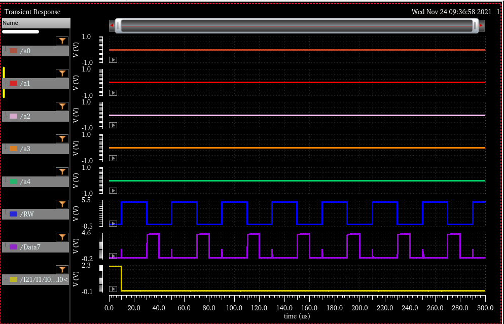
The
following screenshots
show the simulation setup/results showing the Register File. In
the setup we are accessing address 00000 by setting all the a inputs to
gnd. Along with that the data pins are set to gnd with only data
7 pin and RW being pulsed. This is to see if the RW pin is
reading and writing the data value into the SRAM cell correctly.
Unfortunately I was unsuccessful in getting the SRAM cell to work
correctly based on the inputs of the register file.
The contents of this project may be downloaded here
Return to Student Lab Reports
Return to Class Webpage