Lab 7 - EE 421L Fall 2021
Authored
by: Anthony Torres
Email: torrea20@unlv.nevada.edu
Due Date: November 3, 2021
Lab Description
This laboratory assignment is using buses and arrays of word inverters, muxes and high-speed adders.
Pre-Lab
The
pre-lab goes over the key point in Tutorial 5 which is the schematic
and layout view of a ring oscillator which is shown by the following
screenshots.
Main Lab
This
lab goes over how to use buses and arrays with various differnt gates.
Those gates being NAND, NOR, AND, OR and a inverter, along with
the logic gates a 2 to 1 DEMUX/MUX is also created and simulated to
show that they work. The last part of the lab is creating a full
adder that will be used to draft a 8-bit adder. The points below
give a brief description of what to expect from each part.
- Schematic and symbol of 4-bit inverter followed by simulation setup and results.
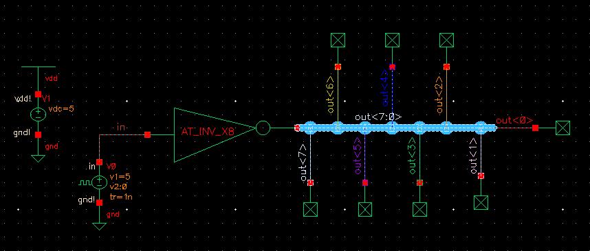
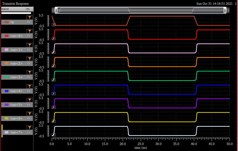
- Schematic and symbol of 8-bit inverter followed by simulation setup and results.
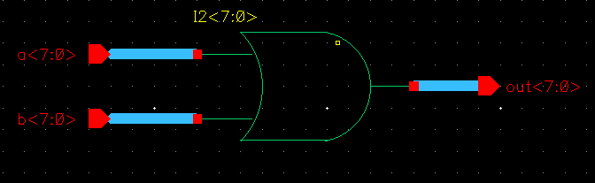
-
Schematic and symbol of 8-bit NAND gate followed by simulation setup
and results. That cover the four possible inputs(00,01,10,11).
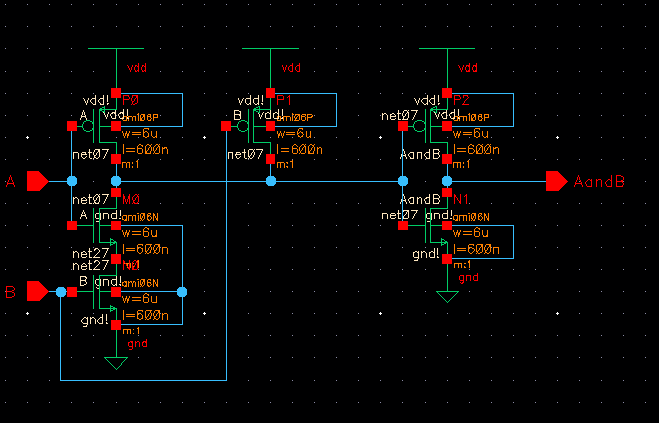
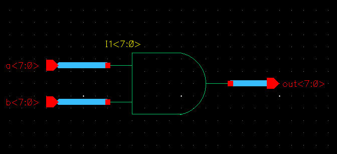
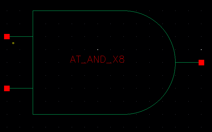
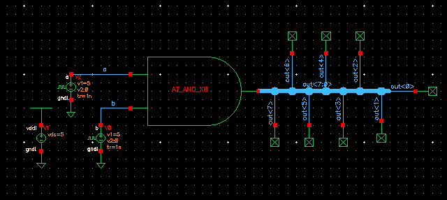
- Schematic and symbol of
8-bit AND gate followed by simulation setup and results. That cover
the four possible inputs(00,01,10,11).
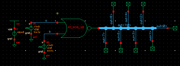
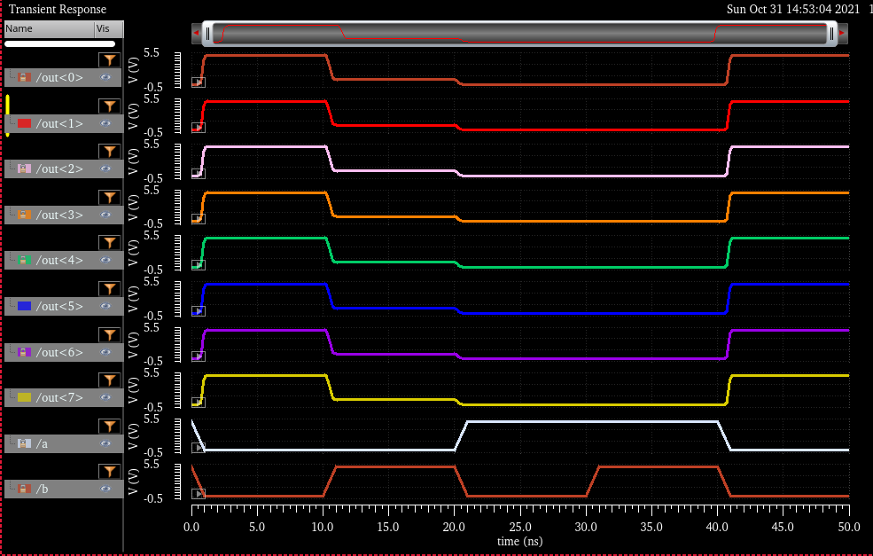
- Schematic and symbol of
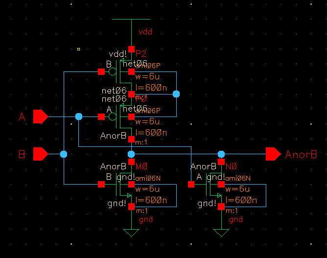
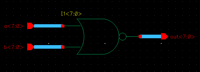
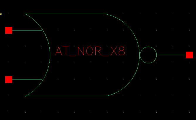
8-bit NOR gate followed by simulation setup and results. That cover
the four possible inputs(00,01,10,11).
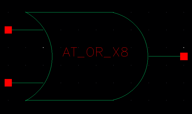
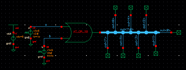
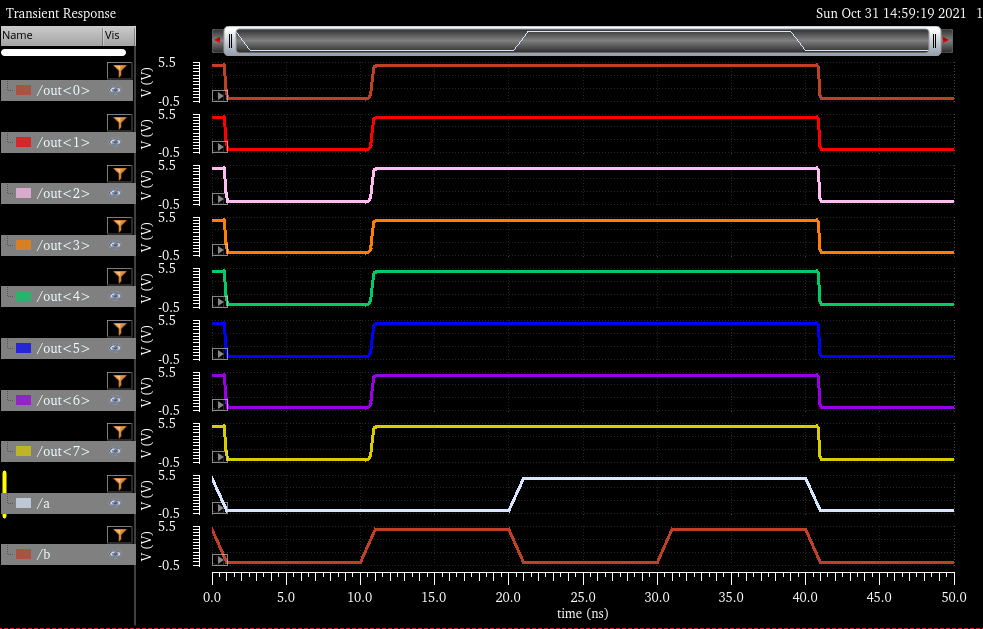
- Schematic and symbol of
8-bit OR gate followed by simulation setup and results. That cover
the four possible inputs(00,01,10,11).
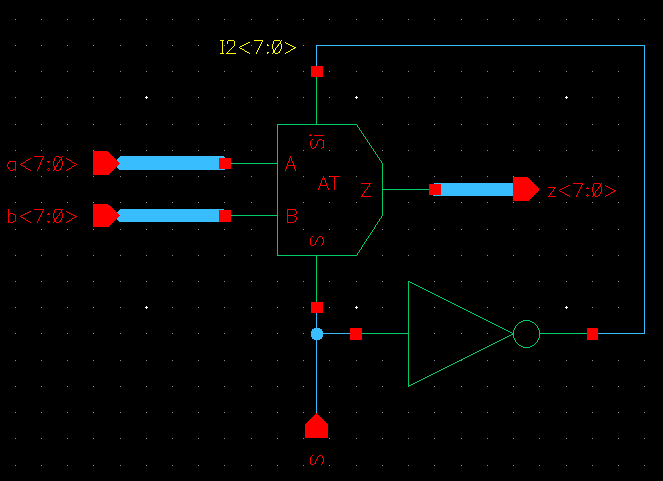
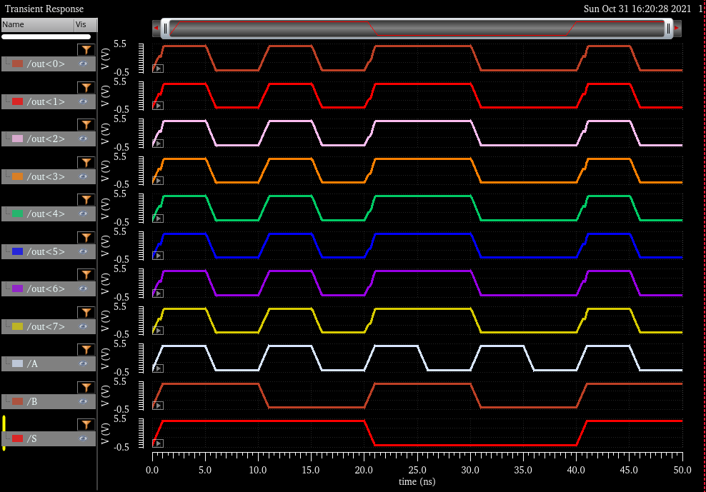
- Schematic and symbol of a 2 to 1 Mux followed by simulation setup and results.
- Schematic and symbol of
8-bit 2 to 1 Mux followed by simulation setup and results. That cover
the eight possible inputs(000,001,010,011,100,101,110,111).
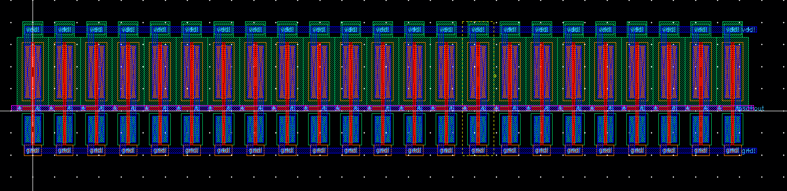
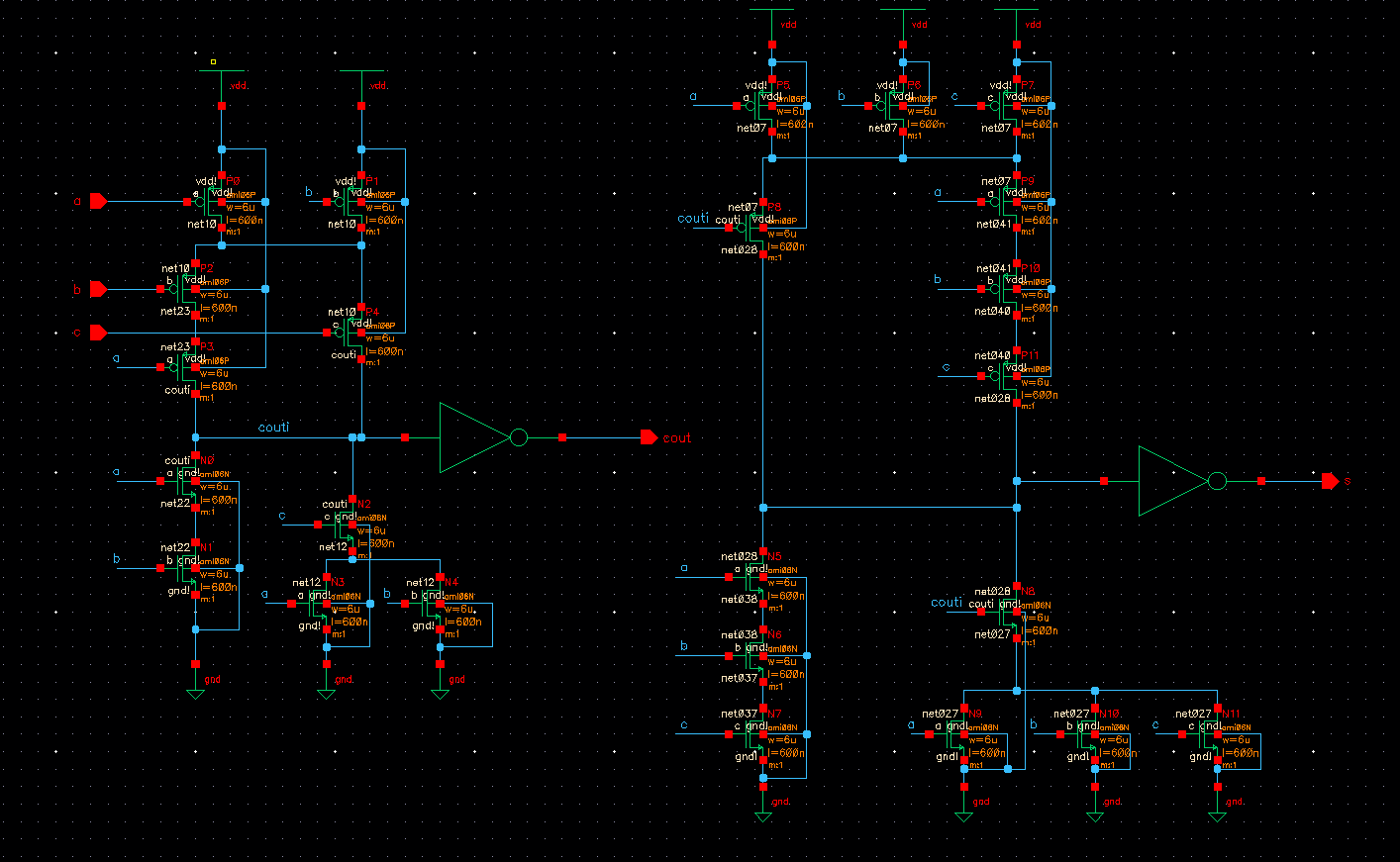
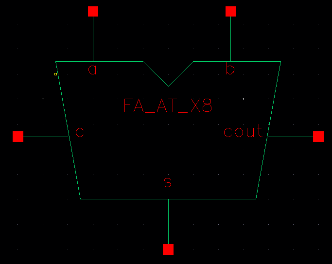
- Schematic, symbol and layout of a full-adder followed by simulation setup and results.
- Schematic, symbol and layout of 8-bit full-adder followed by simulation setup and results. That cover
the eight possible inputs(000,001,010,011,100,101,110,111).
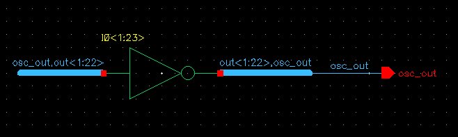
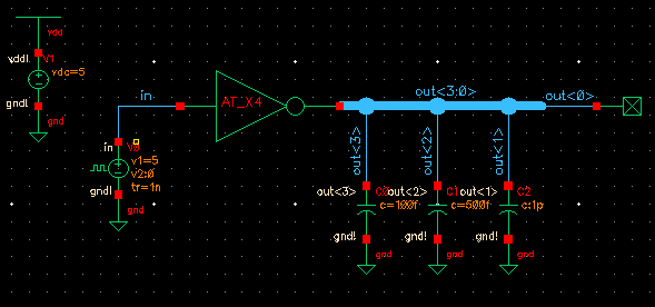
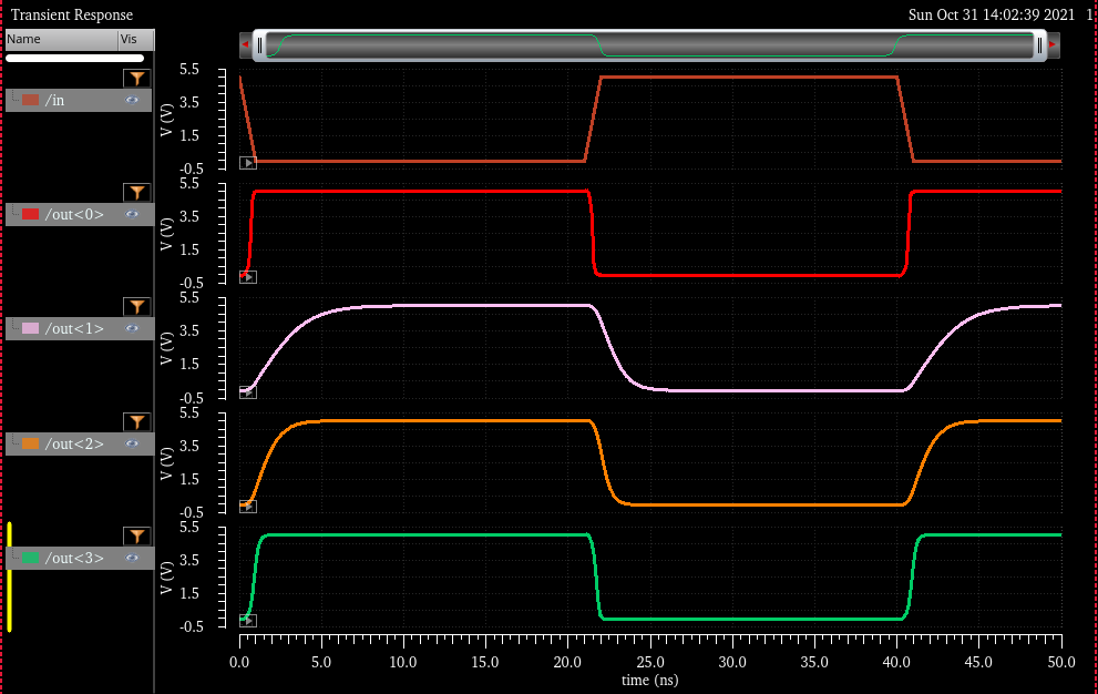
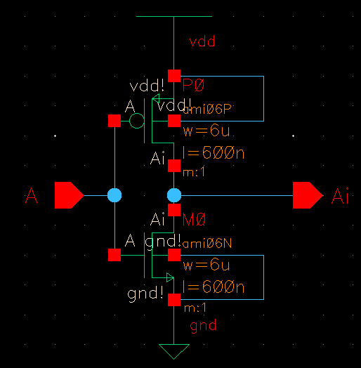
4-bit Inverter
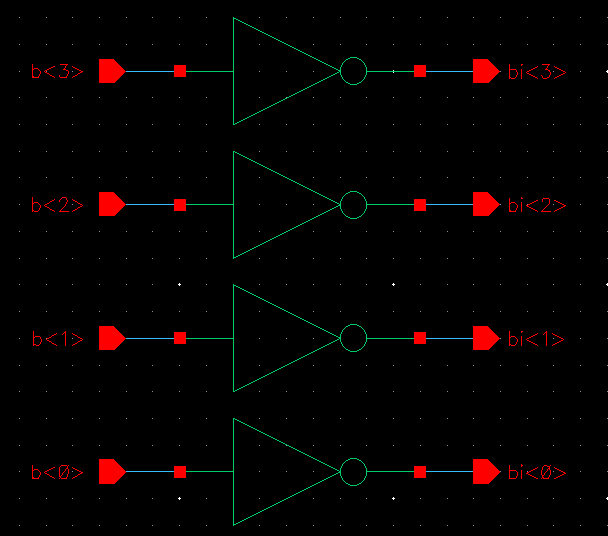
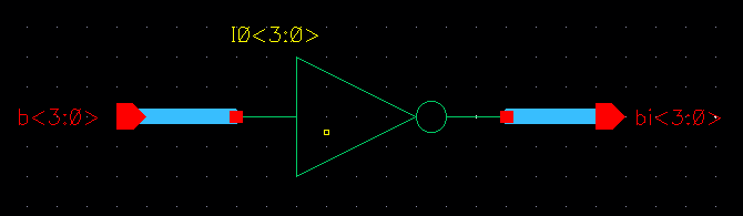
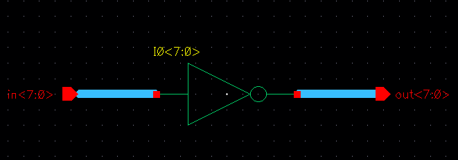
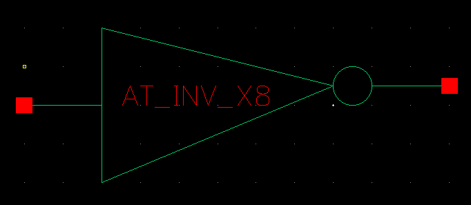
8-bit Inverter
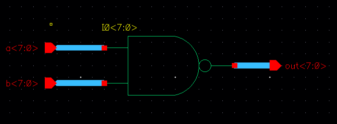
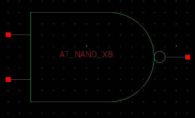
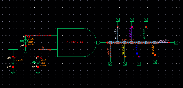
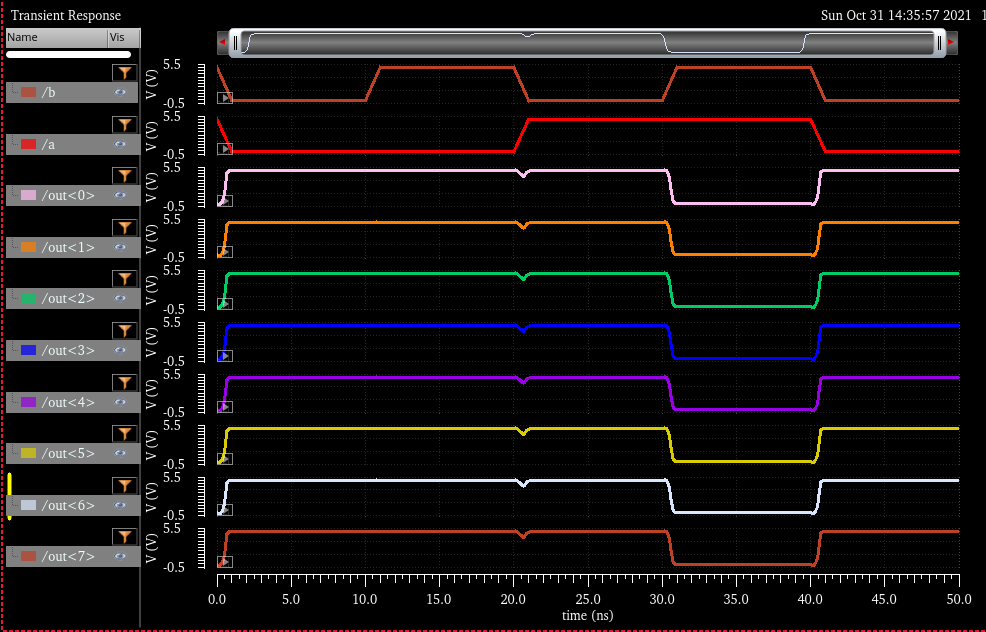
8-bit NAND gate
8-bit AND gate
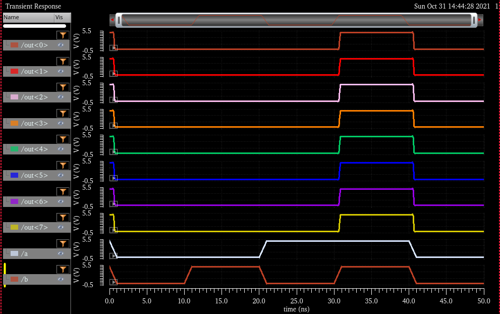
8-bit NOR gate
8-bit OR gate
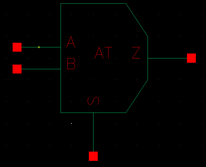
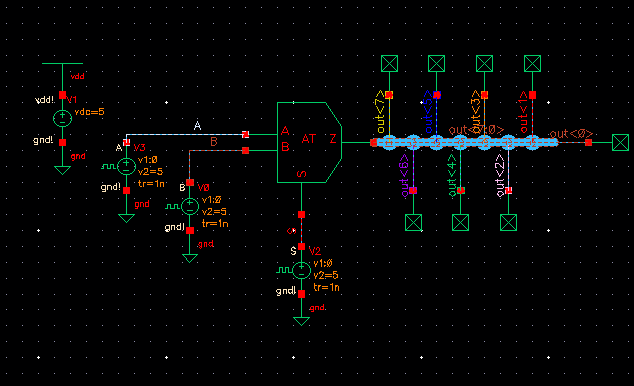
2 to 1 MUX
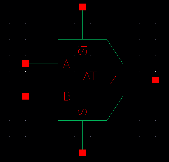
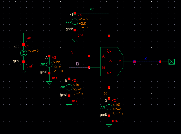
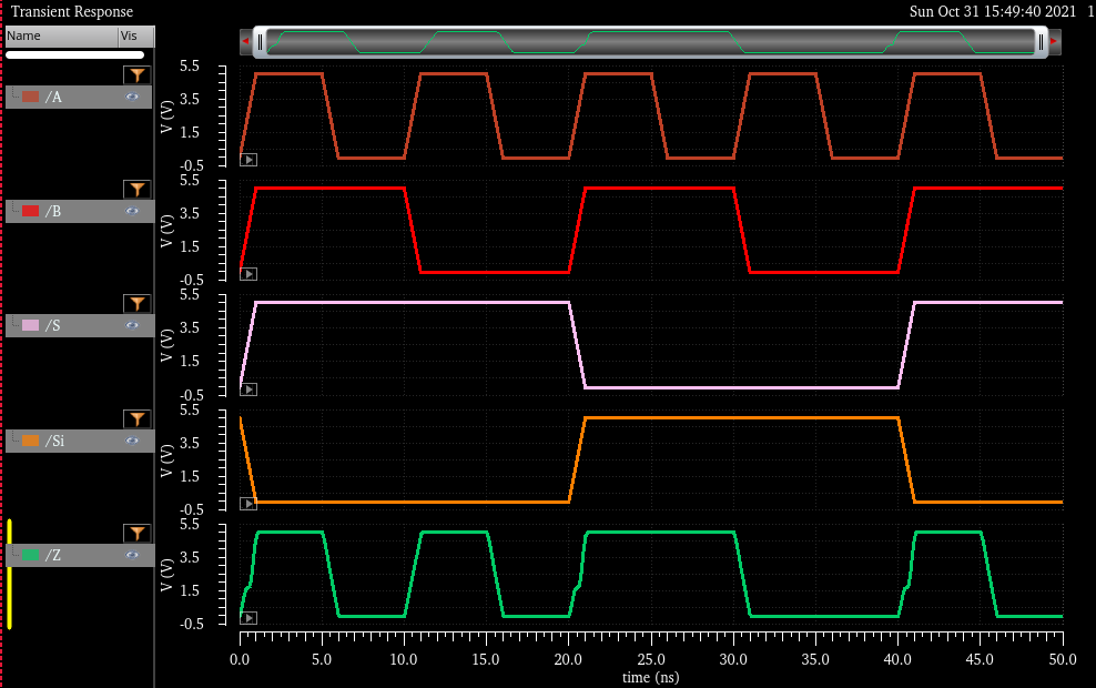
8-bit 2 to 1 MUX(S pin includes an inverter to remove one input)
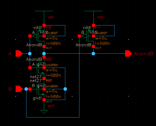
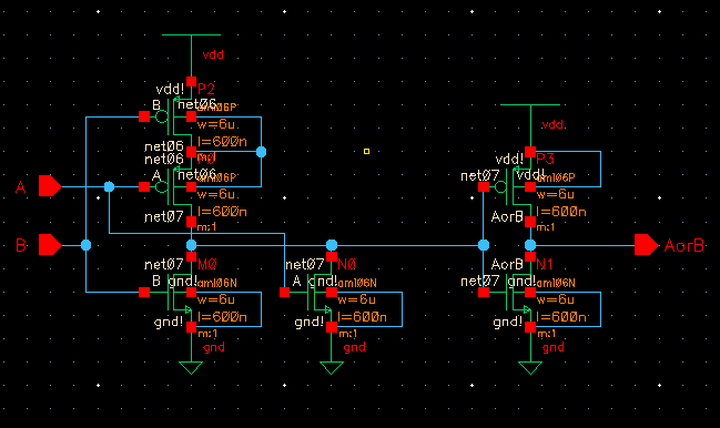
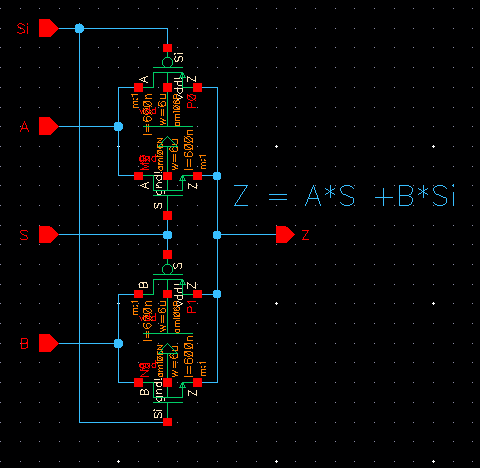
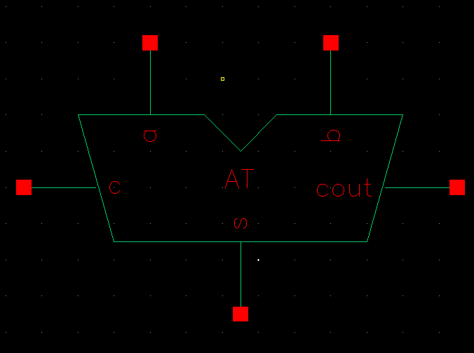
The
next part of the lab is to draft the schematic of the full adder seen
in Fig.12.20 in the CMOS book. Using that schematic a symbol and
layout with a LVS check was done and the following screenshots show the
results.
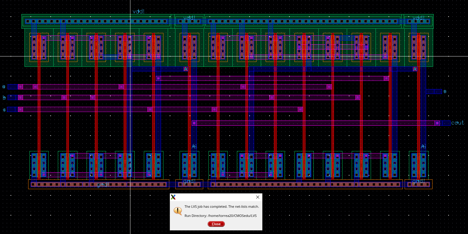
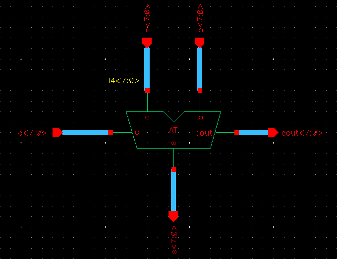
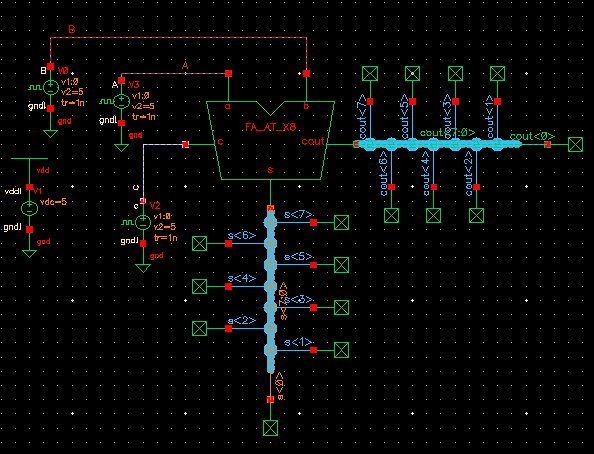
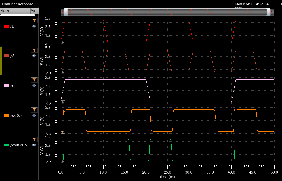
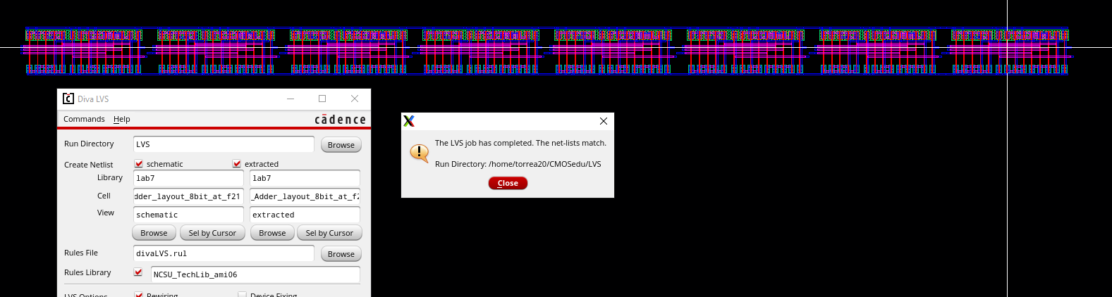
The final part of the lab is to create a 8-bit Full Adder using the
created symbol. The following screenshots show the schematic,
symbol simulation setup and results that cover the 8 possible inputs
being(000,001,010,011,100,101,110,111). Along with that the
layout was created using the full adder and the screenshot below show
the layout with the LVS check to ensure the LVS match.
The following lab can be downloaded here
Return to Student Lab Reports
Return to Class Webpage