Lab 6 - EE 421L Fall 2021
Authored
by: Anthony Torres
Email: torrea20@unlv.nevada.edu
Due Date: October 20, 2021
Lab Description
This laboratory assignment Design, layout and simulation of a CMOS NAND gate, XOR gate and Full-Adder.
Pre-Lab
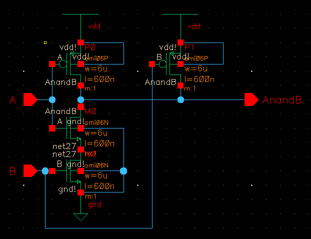
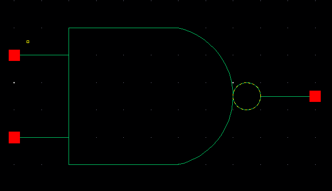
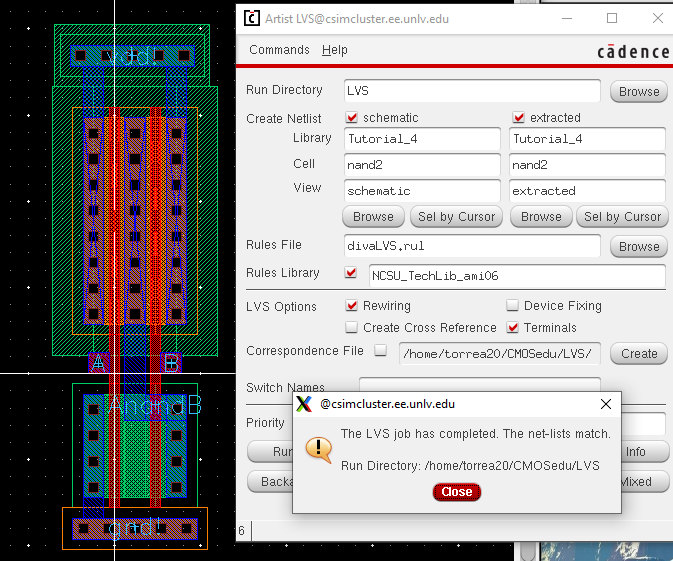
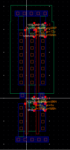
The
pre-lab goes over the key point in Tutorial 4 which is the design and
layout of a CMOS NAND gate. The following screenshots show the
schematic, symbol, layout and extractred view of the CMOS NAND gate followed by
a LVS check to ensure the netlist match.
Main Lab
The
lab is based around drafting the schematics of the 2-input NAND and XOR
gates using 6u/.6u MOSFETs. From those gates a full adder will be
created followed by layout and simulations of each circuit. The
following points give a brief description of what to expect.
- Schematics and simulation of 2 input NAND gate that show the 4 possible inputs (00,01,10,11).
- Schematics, layout and simulation of 2 input XOR gate that show the 4 possible inputs (00,01,10,11).
- Schematics, layout and simulation of full adder that show the 8 possible inputs (000,001,010,011,100,101,110,111).
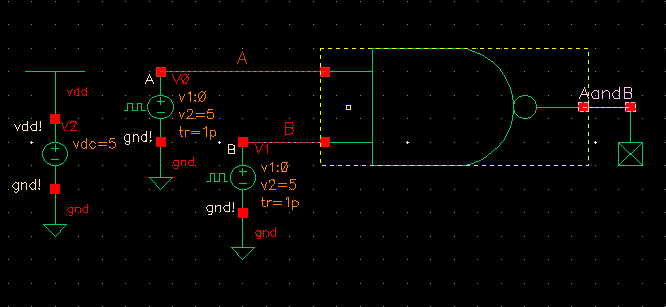
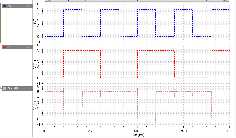
The
schematic, layout and extracted view of the 2 input NAND gate can be
found in the pre-lab. The following screenshots below show the
setup and simulation of the 2 input NAND gate with an A input that has
a pulse source that has a period of 20nS and a B input that has a
period of 40nS. The reason this is done is so that the four
possible outputs may be shown.
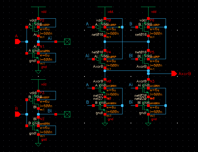
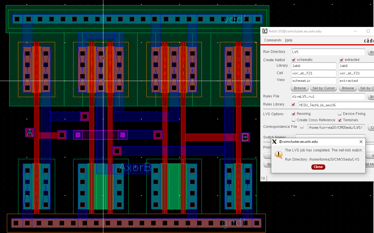
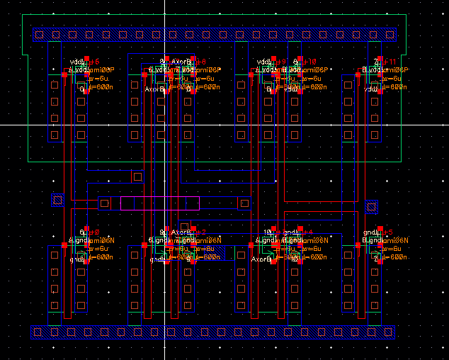
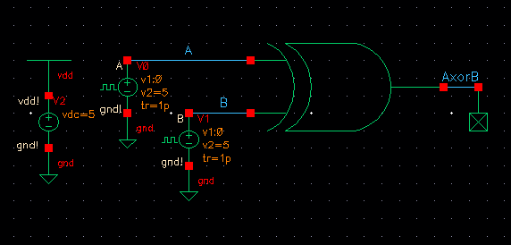
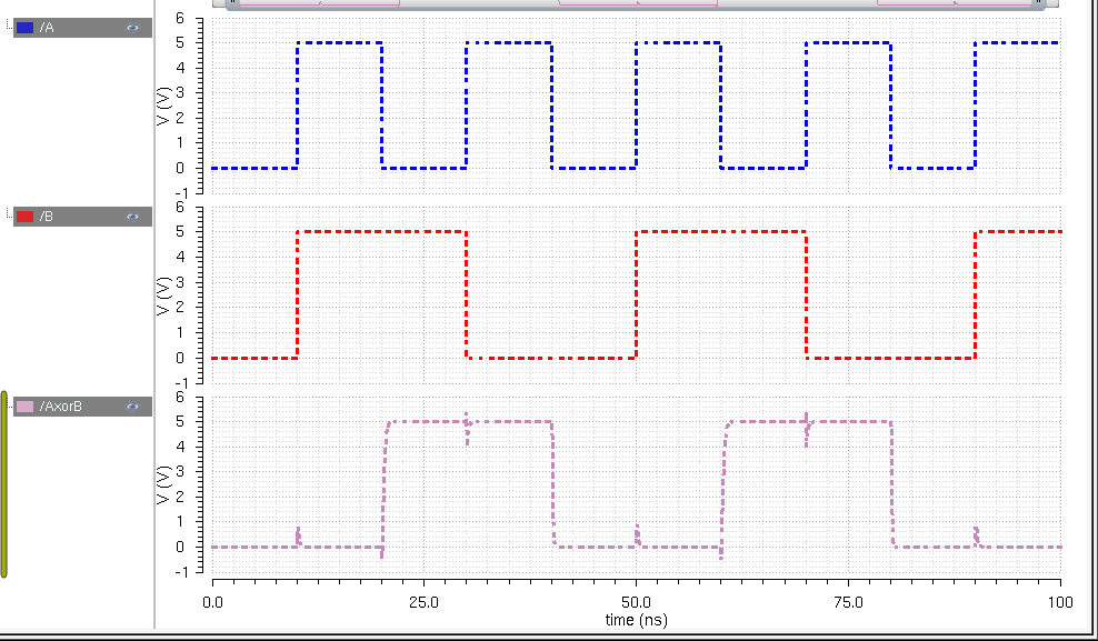
The schematic, layout and extracted view
of the 2 input XOR gate can be found below followed by the LVS check to ensure the netlist match.
The following
screenshots below show the setup and simulation of the 2 input XOR
gate with an A input that has a pulse source that has a period of 20nS
and a B input that has a period of 40nS. The reason this is done
is so that the four possible outputs may be shown.
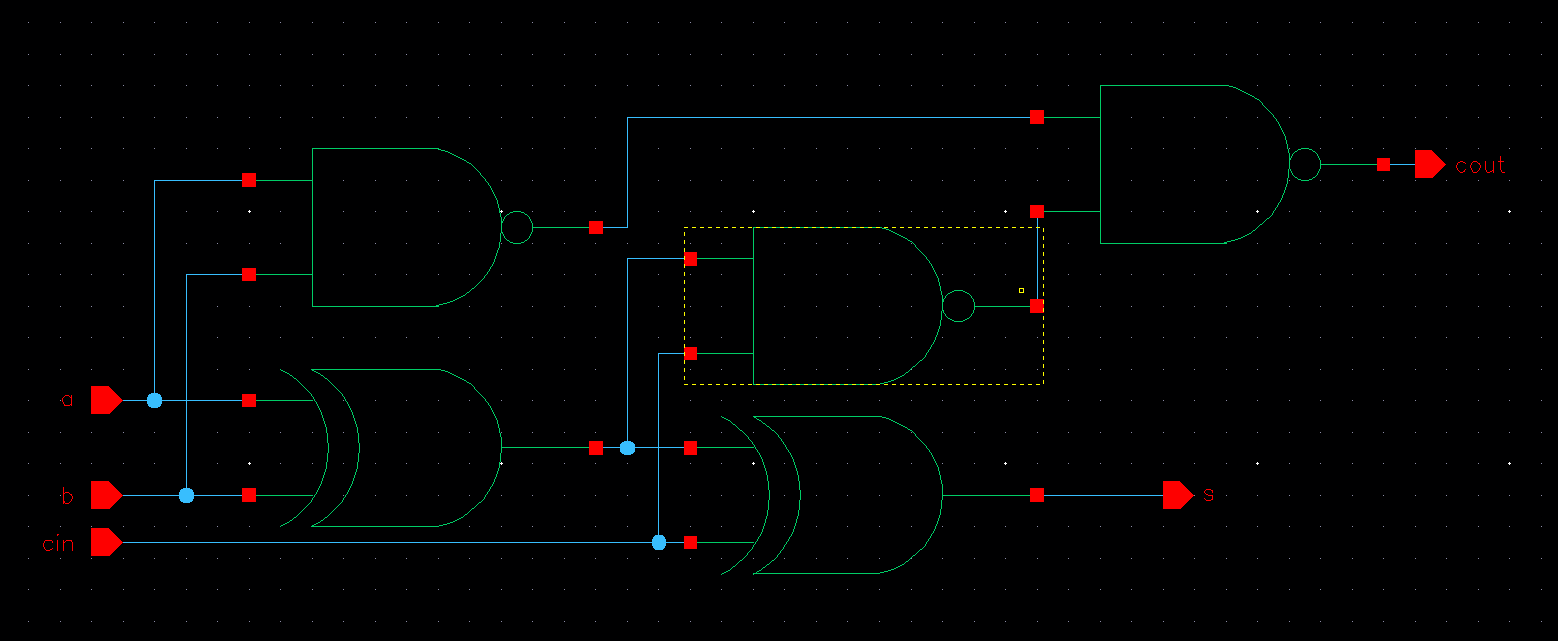
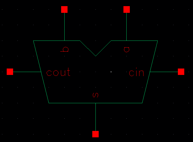
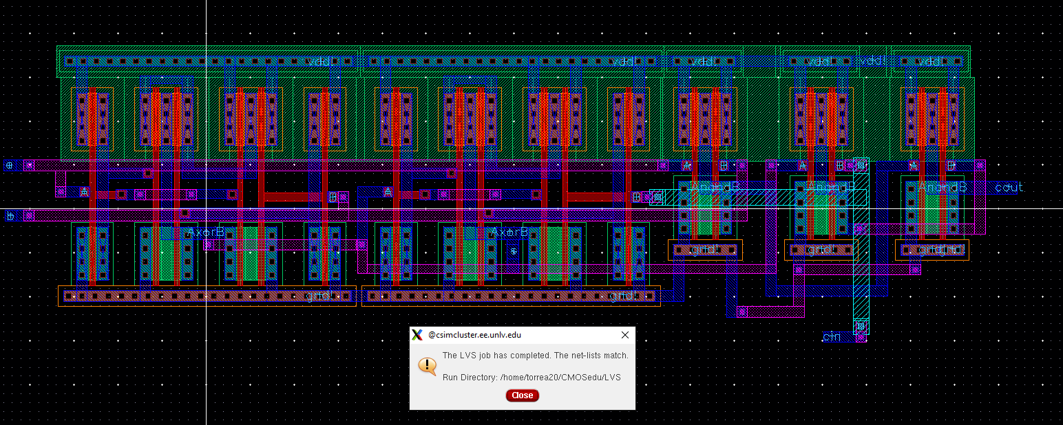
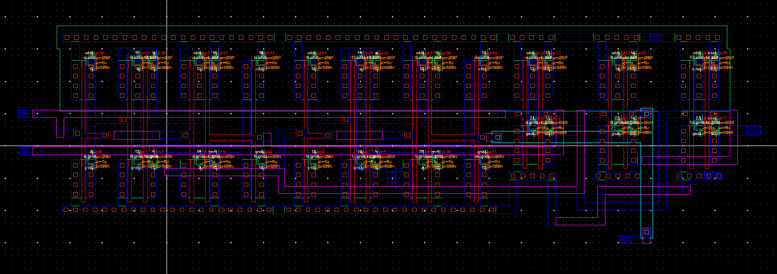
The schematic, layout and extracted view
of the full adder can be found below followed by the LVS check to ensure the netlist match.
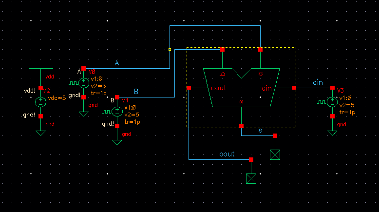
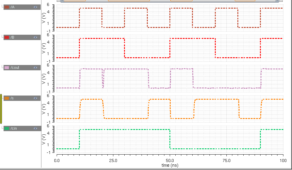
The
following
screenshots below show the setup and simulation of the full adder with
an A input that has a pulse source that has a period of 20nS, a B input
that has a period of 40nS and the cin input that has a period of 80ns.
The reason this is done
is so that the eight possible outputs may be shown.
The following lab contents may be downloaded here
Return to Student Lab Reports
Return to Class Webpage