Lab 5 - EE 421L Fall 2021
Authored
by: Anthony Torres
Email: torrea20@unlv.nevada.edu
Due Date: October 6, 2021
Lab Description
This laboratory assignment Design, layout and simulation of a CMOS inverter.
Pre-Lab
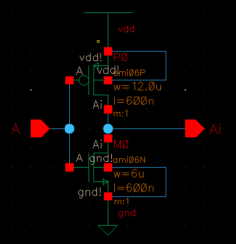
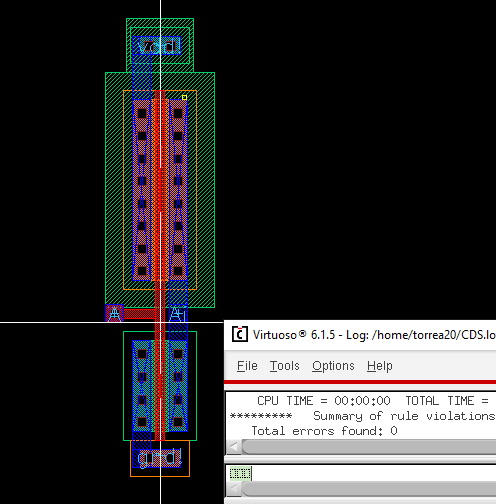
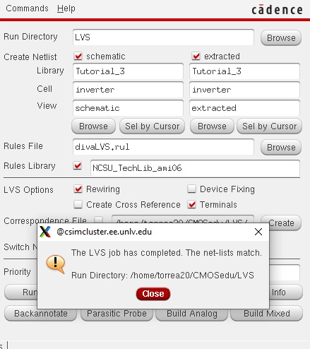
The
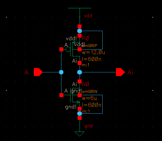
pre-lab is to go through Tutorial 3. The following screenshots
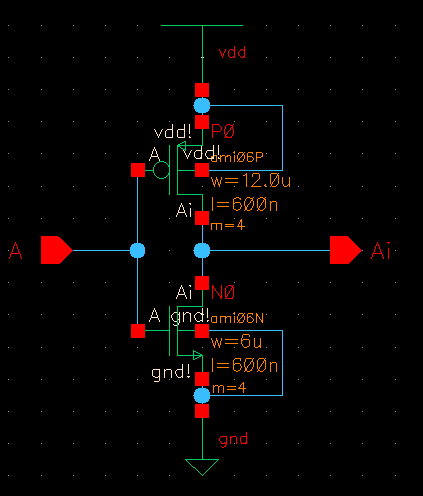
are the schematic of a CMOS inverter which is made using a PMOS and
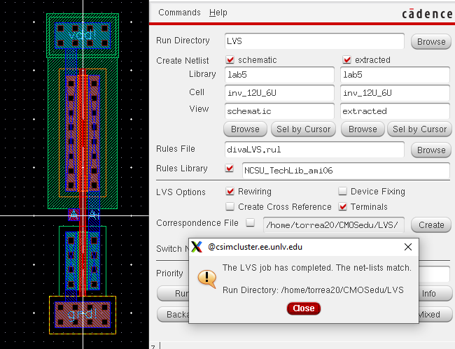
NMOS device followed by the layout and extracted view. Lastly the
LVS check is included to ensure the net-list match.
Main Lab
This
lab is based around drafting the schematic, layout and symbol for two
different inverters as well as running simulations with a varying load.
The following points are a brief description of each part.
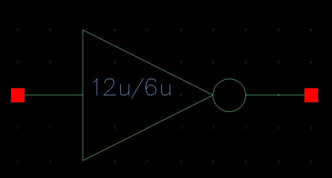
- Schematic, layout and symbol of CMOS inverter with a size of 12U/6U
- Setup and simulation results of the 12U/6U CMOS inverter with a varying capacitor load of 100f,1p,10p,100p.
- Schematic, layout and symbol of CMOS inverter with a size of 48U/24U
- Setup and simulation results of the 48U/24U CMOS inverter with a varying capacitor load of 100f,1p,10p,100p.
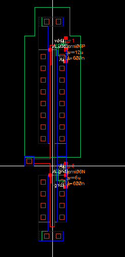
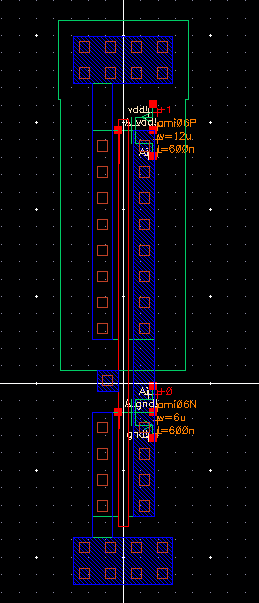
Shown
below is the schematic, symbol, layout and extracted view for the
12U/6U which was apart of the pre-lab. Included with the layout
is the LVS check to ensure the netlist match.
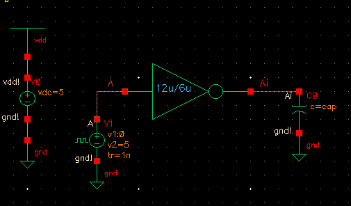
Shown
below is the circuit setup to simulate the 12U/6U CMOS inverter with
varying loads. The inverter symbol is used instead of having the
inverter schematic along with the capactive load being given a variable
name "cap" and will be varying from (100f, 1p, 10p, 100p) Farads. This
is done by going to (Tools - Parameteric Anaysis) so that the outputs
will be on the same graph.
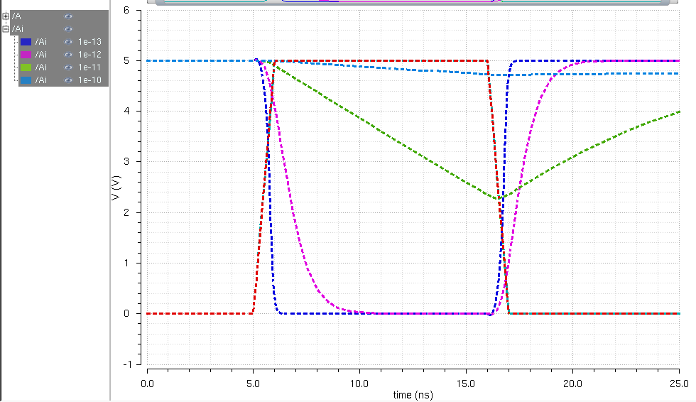
Spectre Simulation
- A, input(Red) is a pulse source going from 0 to VDD.
- Ai, output(Blue) is the 100pF load shows the inverter working correctly
- Ai, output(Pink) is the 1pF load shows the inverter working correctly however it has a larger delay
- Ai, output(Green) is the 10pF load shows the inverter not working correctly because the capacitor is charging and discharging.
- Ai, output(Light Blue) is the 100pF load show the inverter not working correctly because the capacitor is charging.
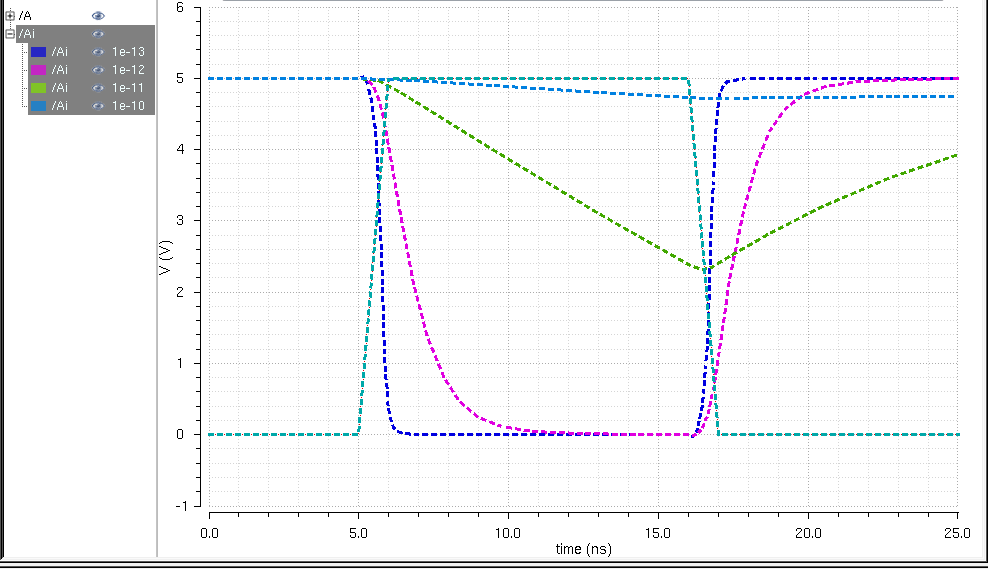
UltraSim Simulation - No noticable difference because it is a smaller circuit, as a result the graph is the same as before.
- A, input(Turquoise) is a pulse source going from 0 to VDD.
- Ai, output(Blue) is the 100pF load shows the inverter working correctly
- Ai, output(Pink) is the 1pF load shows the inverter working correctly however it has a larger delay
- Ai, output(Green) is the 10pF load shows the inverter not working correctly because the capacitor is charging and discharging.
- Ai, output(Light Blue) is the 100pF load show the inverter not working correctly because the capacitor is charging.
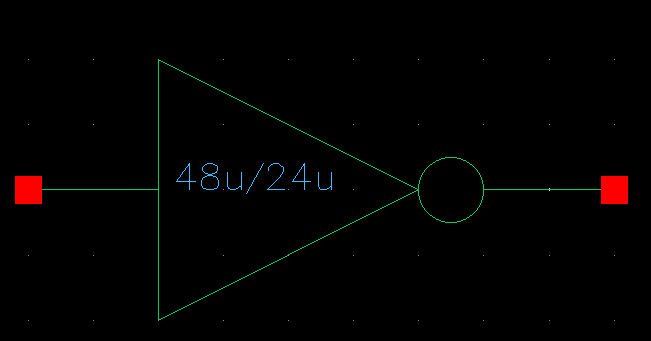
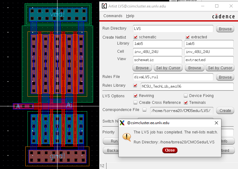
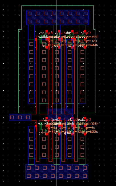
Shown
below is the schematic,
symbol, layout and extracted view for the 48U/24U this was done by
having a device multiplier m = 4. Included with the layout is the
LVS check to ensure the
netlist match.
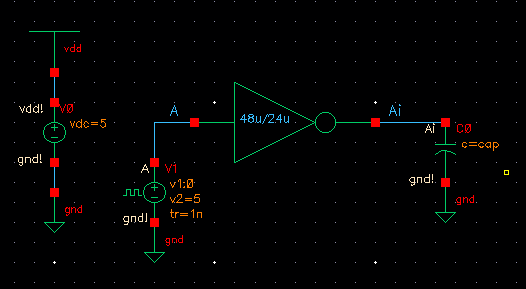
Shown below is the circuit
setup to simulate the 48U/24U CMOS inverter with varying loads. The
inverter symbol is used instead of having the inverter schematic along
with the capactive load being given a variable name "cap" and will be
varying from (100f, 1p, 10p, 100p) Farads. This is done by going to
(Tools - Parameteric Anaysis) so that the outputs will be on the same
graph.
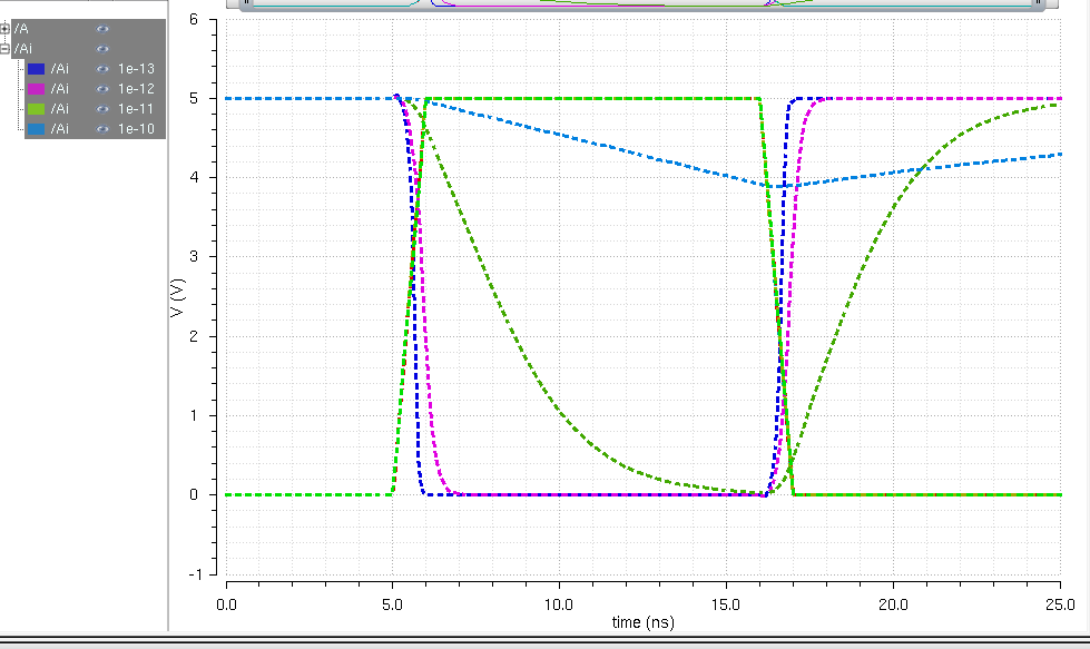
Spectre Simulation
- A, input(Light Green) is a pulse source going from 0 to VDD.
- Ai, output(Blue) is the 100pF load shows the inverter working correctly
- Ai, output(Pink) is the 1pF load shows the inverter working correctly however it has a larger delay
- Ai, output(Green) is the 10pF load shows the inverter not working correctly because the capacitor is charging and discharging.
- Ai, output(Light Blue) is the 100pF load show the inverter not working correctly because the capacitor is charging.
UltraSim Simulation - No noticable difference because it is a smaller circuit, as a result the graph is the same as before.
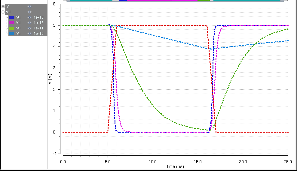
- A, input(Red) is a pulse source going from 0 to VDD.
- Ai, output(Blue) is the 100pF load shows the inverter working correctly
- Ai, output(Pink) is the 1pF load shows the inverter working correctly however it has a larger delay
- Ai, output(Green) is the 10pF load shows the inverter not working correctly because the capacitor is charging and discharging.
- Ai, output(Light Blue) is the 100pF load show the inverter not working correctly because the capacitor is charging.
The following lab contents may be downloaded here
Return to Student Lab Reports
Return to Class Webpage