Lab 4 - EE 421L Fall 2021
Authored
by: Anthony Torres
Email: torrea20@unlv.nevada.edu
Due Date: September 22, 2021
Lab Description
This laboratory assignment is the IV characteristics and layout of NMOS and PMOS devices
Pre-Lab
- This prelab goes through the main parts of Tutorial 2
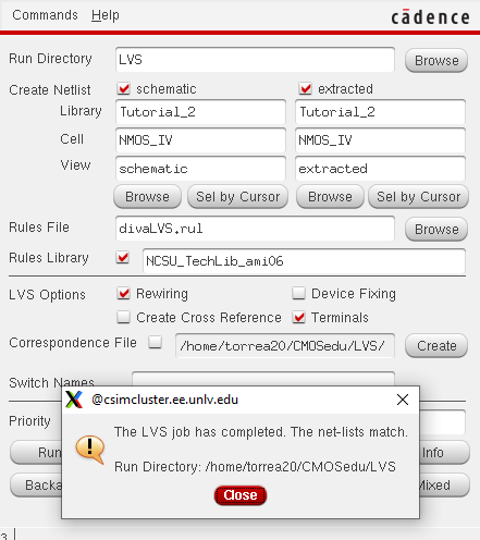
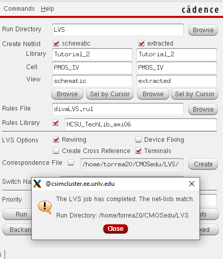
The first part is the layout of an NMOS device which is created with a nmos, ptap and m1_poly
layouts. After the layout it was DRC checked and extracted so
that the LVS may be checked to find if the net-list match. After
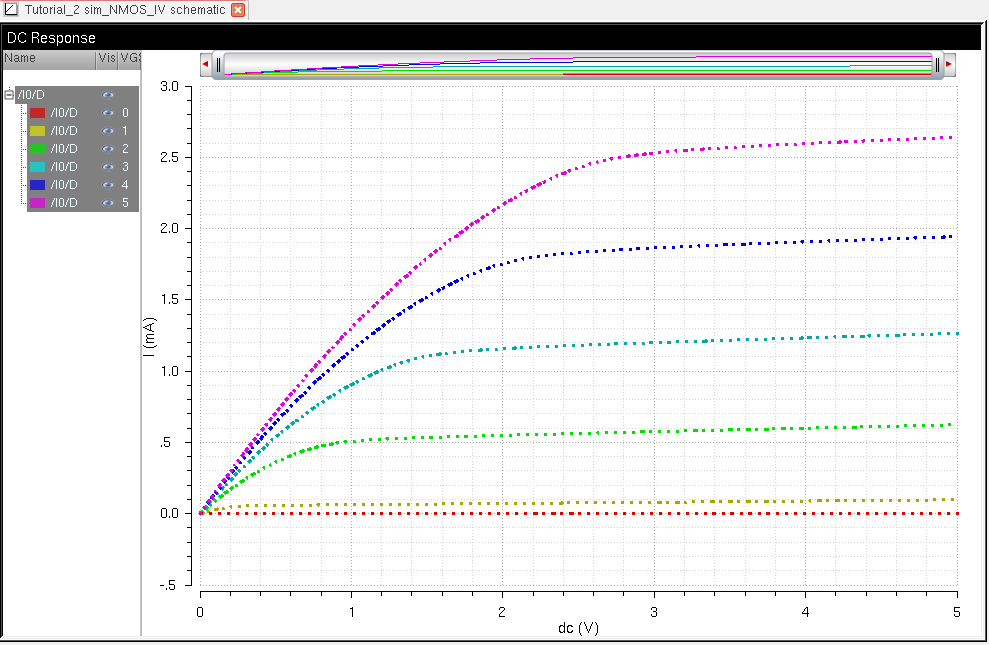
that the NMOS was sim to check the IV curves as VGS changes from 0 to 5
V.
The
second part of is the layout of the PMOS device and getting the
extracted view so that the layout may be LVS checked to ensure the
net-list match. Next the PMOS devices was simulated to check the
IV curves as VSG changes from 0 to 5V.
Main Lab
This
lab is based around the IV characteristics and layout of NMOS and PMOS
devices. The following points below give a brief description of
what is included in the lab.
- IV characterics of NMOS device with a sweeping VDS and VGS
- IV characterics of PMOS device with a sweeping VSD and VSG
- Layout of NMOS and PMOS devices including probe pads connected to terminals
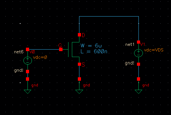
The
first part of the Lab is showing the IV characteristics of the NMOS
device. Below is the schematic that is used to simulate the IV
curves.
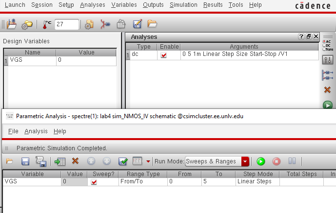
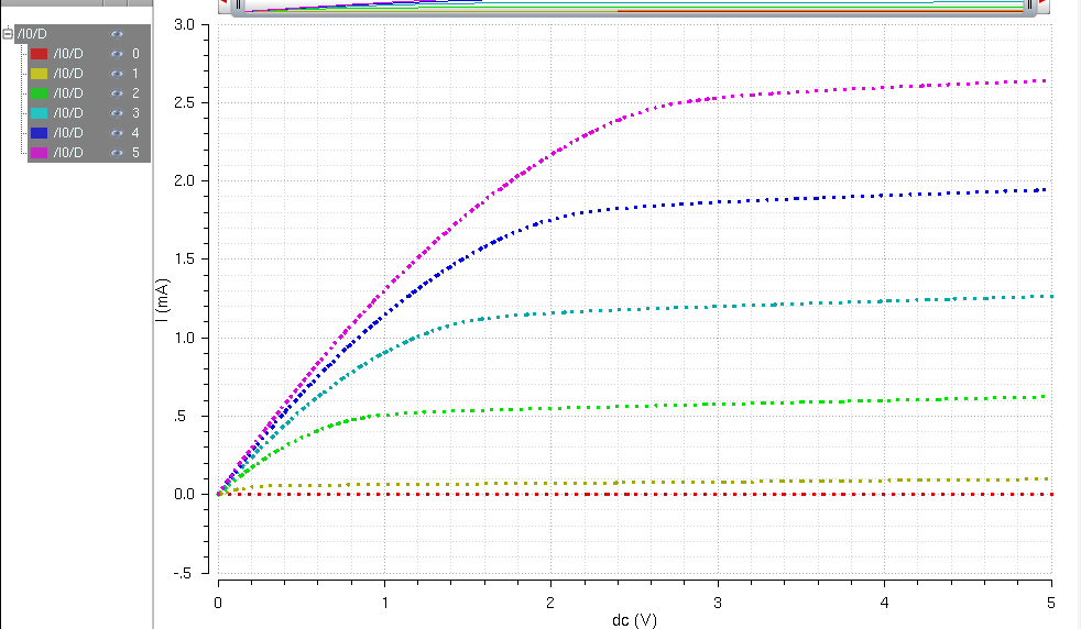
Shown
below is the setup for the simulation in this case VDS was swept from 0
to 5V with 1mV steps while VGS was changing from 0 to 5V.
The result shows the drain current as those values are swept.
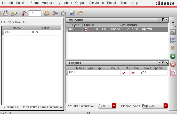
The
next simulation is when VGS is swept from 0 to 2V with 1mV steps while
VDS is held at 100mV. The screenshots below include the setup and
result.
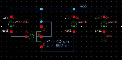
The next part of the Lab is
showing the IV characteristics of the PMOS device. Below is the
schematic that is used to simulate the IV curves.
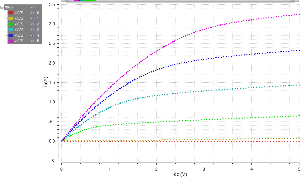
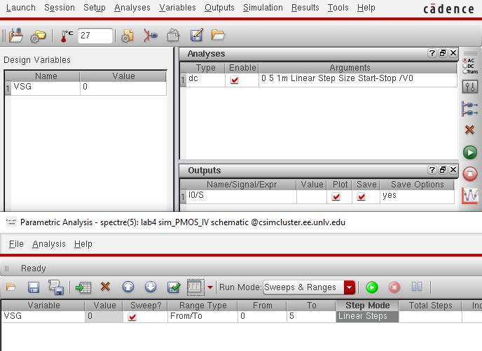
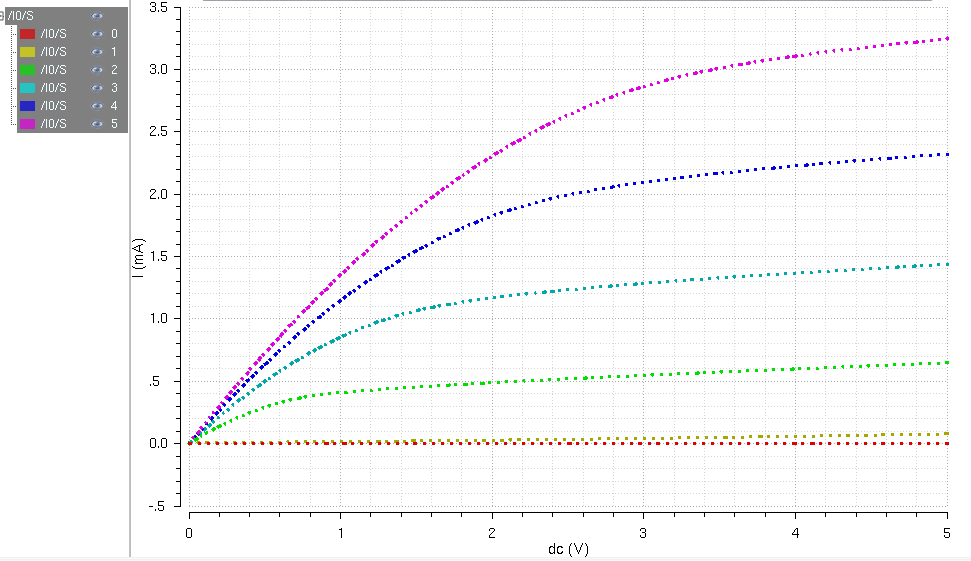
Shown below is the setup for
the simulation in this case VSD was swept from 0 to 5V with 1mV steps
while VSG was changing from 0 to 5V. The result shows the drain
current as those values are swept.
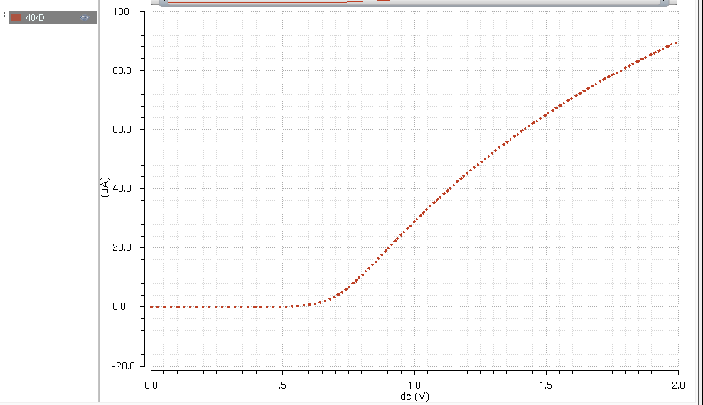
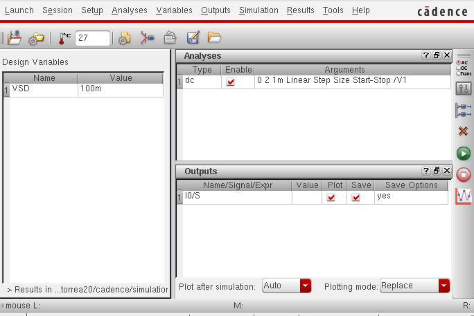
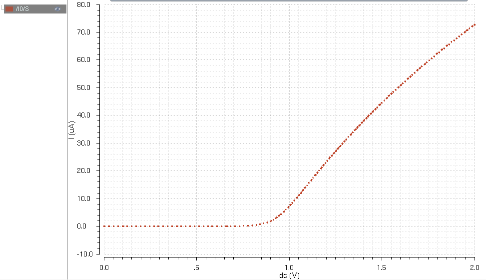
The next simulation is when
VSG is swept from 0 to 2V with 1mV steps while VSD is held at 100mV.
The screenshots below include the setup and result.
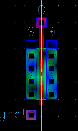
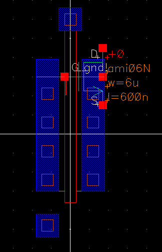
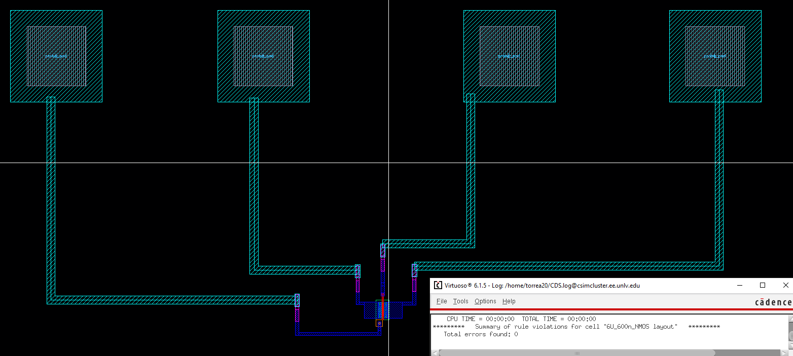
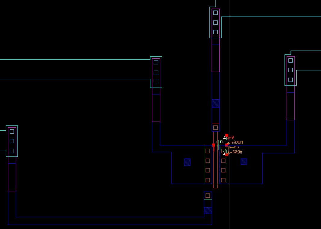
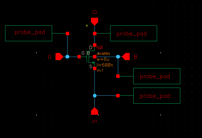
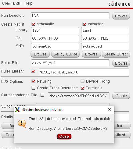
The
next part of the lab is to layout a NMOS device with probe pads
connected to the gates. The screenshots below show the layout
created with a DRC to ensure no erros. Followed by the extracted
view, schematic and LVS check to ensure the net-list match.
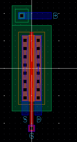
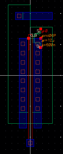
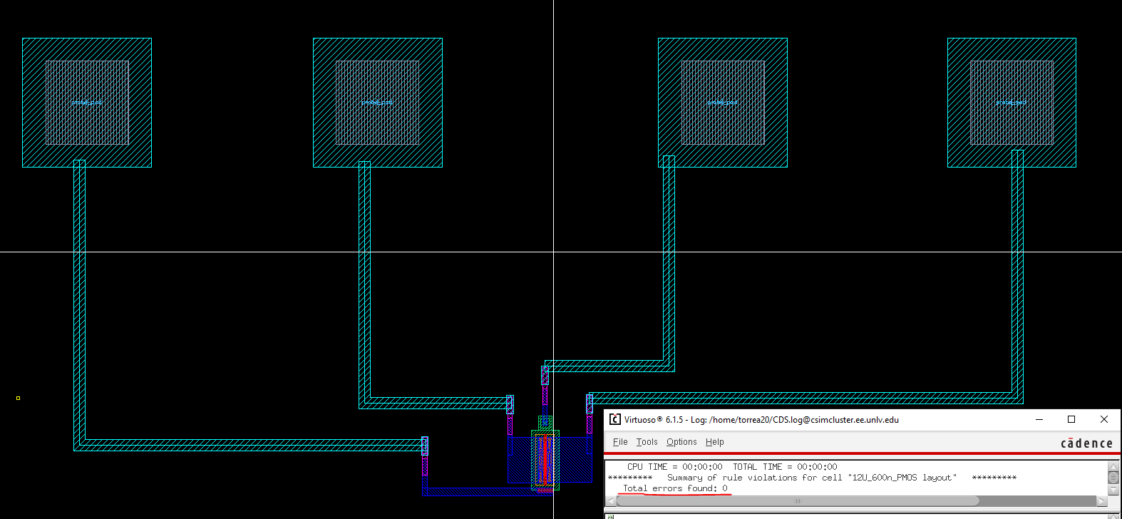
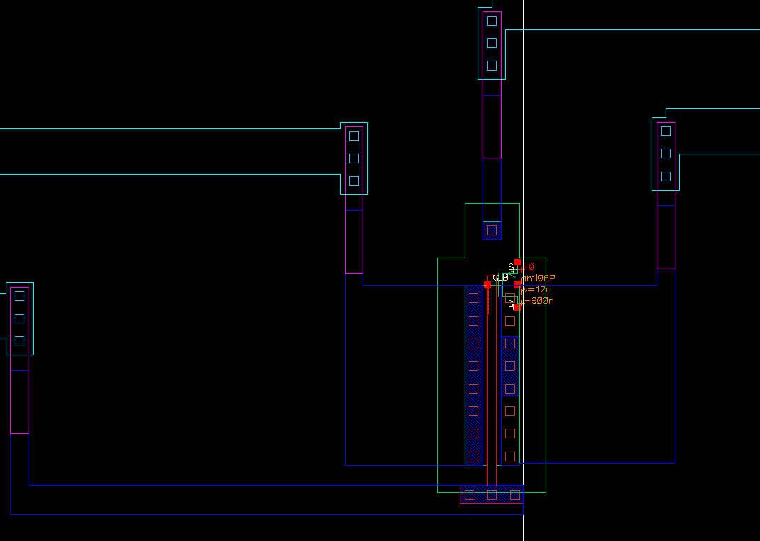
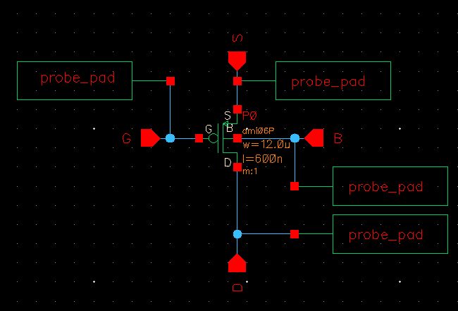
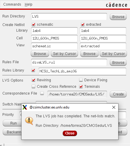
The final part of the lab is
to layout a PMOS device with probe pads connected to the gates. The
screenshots below show the layout created with a DRC to ensure no
erros. Followed by the extracted view, schematic and LVS check to
ensure the net-list match.
The contents of this lab may be downloaded here
Return to Student Lab Reports
Return to Class Webpage