Lab 4 - EE 421L
Authored
by Jimmy Ruangnol,
(ruangnol@unlv.nevada.edu)
September 19, 2021
Lab Description
The
purpose of this lab is to analyze I-V curves of MOSFET devices, such
as, NMOS and PMOS transistors. These devices would have three terminals
labeled as: gate, drain, and source. The current is determined by the
votlage that flows between the drain and source. The voltage between
the gate and source can be determine as well. We will be using
parametric analyses to see different linear steps of the curves for the
MOSFET. Students will also create layouts for NMOS and PMOS devices.
Pre-lab work
- Back-up all of your work from the lab and the course.

- Go through Tutorial 2 seen here.
Lab
After
going through tutorial 2, students should be familiar with creating
NMOS and PMOS transistors. For the first part of the lab, we need to
generate different responses from the MOSFET devices through schematics
and simulations.
The NMOS and PMOS devices are available under the NCSU_Analog_Parts library.
We
will be simulating for a NMOS and PMOS response of ID vs VDS and ID vs
VSD. For an NMOS device it will be for VGS, from 0V to 5V in 1V steps.
The NMOS device will utlilized a 6um/600nm width to length ratio. Below
is the simulation standards, VGS for NMOS and VSG for PMOS.

To simulate in linear steps we need to set the criteria of a parametric analysis.

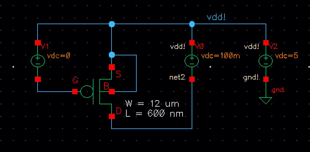
For an PMOS device it will be for VGS, from 0V to 5V in 1V steps. The
PMOS device will utlilized a 12um/600nm width to length ratio. This
will measure for the VSD in increments of 0V to 5V in 1V steps.
Next
we will be simulating for ID vs VGS of an NMOS device of 100mV. It will
be from 0V to 2V in 1mv steps with the same measurements of the NMOS
transistor above. Below is the crieteria for the next simulations.


Next we will be simulating
for ID vs VSG of an PMOS device of 100mV. It will be from 0V to 2V in
1mv steps with the same measurements of the PMOS transistor above.
Layout of MOSFETs
Now
we will create the layout of the MOSFET devices with the intent of
connecting these to test pads. In tutorial 2, it provides step by step
instructions of creating the NMOS and PMOS layout. The NMOS will have a
measurement of 6u/0.6u and the PMOS will have 12u/0.6u. Check the layouts with DRC.
NMOS:


PMOS:


MOSFETs to Pads:
We will be connecting the bonding pads to all parts of the MOSFETS. There will be a pad for the gate, source, drain, and base.
Do
no forget to stack m3_m2 and m2_m1 cells on top eachother to create a
connection to the metal3 to metal1 leayers. Pads must be spaced out a
great amount of distance from each other. Verifiy with DRC and then
with LVS.
NMOS:


PMOS:


After the completion of each lab, make sure to back up all your work!

Return to EE 421L Labs