
Lab 8
EE 421L
Kaione Daniels:
Full Adder
10 Bit0DAC
25KΩ N-Well Resistor
Implemented all parts to the chipAssisted with the drafting of the lab report.
Jimmy Ruangnol:
31-stage ring oscillator to drive 20pF load
Voltage Divider
Assisted with the drafting of the lab report.
Ricardo Rodriguez:
NAND and NOR gates
Inverter
PMOS and NMOS transistors
Lab Description:
Prelab:

| Chip Pin # | Pin Description | Comments |
| 1 | A | Full Adder Input |
| 2 | B | Full Adder Input |
| 3 | Cin | Full Adder Input |
| 4 | Cout | Full Adder Output |
| 5 | S | Full Adder Output |
| Chip Pin # | Pin Description | Comments |
| 6 | osc_out | 31-Ring Ocsillator |
| Chip Pin # | Pin Description | Comments |
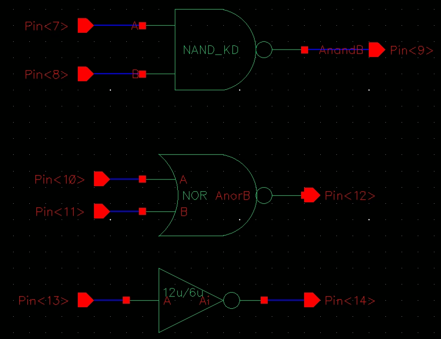
| 7 | A | NAND Input |
| 8 | B | NAND Input |
| 9 | AnandB | NAND Output |
| 10 | A | NOR Input |
| 11 | B | NOR Input |
| 12 | AnorB | NOR Output |
| 13 | A | Inverter Input |
| 14 | Ai | Inverter Output |
| Chip Pin # | Pin Description | Comments |
| 15 | G | PMOS Gate |
| 16 | S | PMOS Source |
| 17 | D | PMOS Drain |
| 18 | B | PMOS Body |
| 19 | G | NMOS Gate |
| 20 | GND | GROUND |
| 21 | S | NMOS Source |
| 22 | D | NMOS Drain |
| Chip Pin # | Pin Description | Comments |
| 23 | 10K | Voltage Divider Input |
| 24 | 25K | Voltage Divider Input |
| 25 | Out | Voltage Divider Output |
| Chip Pin # | Pin Description | Comments |
| 26 | B0 | 10-Bit DAC Input |
| 27 | B1 | 10-Bit DAC Input |
| 28 | B2 | 10-Bit DAC Input |
| 29 | B3 | 10-Bit DAC Input |
| 30 | B4 | 10-Bit DAC Input |
| 31 | B5 | 10-Bit DAC Input |
| 32 | B6 | 10-Bit DAC Input |
| 33 | B7 | 10-Bit DAC Input |
| 34 | B8 | 10-Bit DAC Input |
| 35 | B9 | 10-Bit DAC Input |
| 36 | Vout | 10-Bit DAC Output |
| Chip Pin # | Pin Description | Comments |
| 37 | A | XOR Input |
| 38 | B | XOR Input |
| 39 | AxorB | XOR Output |
| 40 | VDD! | VDD! |

 |  |


| Full Adder Layout | Full Adder Extracted |
 |  |
| Layout of Ring Oscillator |
 |
| Extraction of Ring Oscillator |
 |
| NAND LAYOUT | NAND EXTRACTED |
 |  |
| NOR LAYOUT | NOR EXTRACTED |
 |  |
| INVERTER LAYOUT | INVERTER LAYOUT |
 |  |

| PMOS LAYOUT | PMOS EXTRACTED |
 |  |
| NMOS LAYOUT | NMOS EXTRACTED |
 |  |

 |
 |
 |
| DAC Layout |
 |
| DAC Extraction |
 |
XOR Layout and Extracted:
| XOR Layout | XOR Extraction |
 |  |
This concludes our group's lab 8 test chip design.
The files of the chip can be found here