Lab 4 - EE 421L
Authored
by Ricardo Rodriguez
UNLV E-mail: rodrir15@unlv.nevada.edu
September 22, 2021
Prelab Work:
- Back-up all of
your work from the lab and the course.
- Read through this lab before starting it.
- Go through Tutorial 2 seen here.
Note: In
the simulations in this lab the body of all NMOS devices (the
substrate) should be at ground (gnd!) and the body of all PMOS devices (the
n-well) should be at a vdd! of 5V.
The NMOS and PMOS will both have 4 pins. In our process it will be
assumed that the bulk will be at ground and at Vdd, respectively.
We
must use the nmos4/pmos4 devices in order for our LVS of our schematic and layout of our transistor to match.
The
NMOS transistor will have the dimensions of 6 microns wide and 0.6
microns long. The PMOS will be 12 microns wide and 0.6 microns
long.
NMOS Transistor:
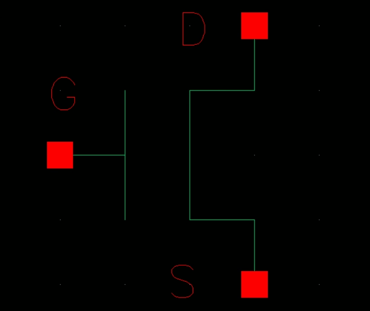
Below is the schematic and symbol for the NMOS. We connect the nmos4
instance to our inputoutput pins of Gate, Drain, and Source.
The
bulk of the transistor is tied directly to ground. Our symbol
simplifies the schematic by just showing the 3 pins that we will be
looking at.

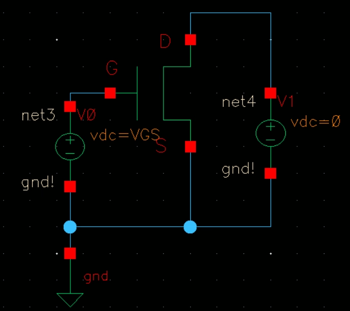
Since
we have our symbol and our NMOS transistor ready to use, we can go
ahead and put it in another schematic for the purpose of simulating.
We can connect our gate to a variable voltage VGS, the source to ground, and our drain to a voltage of 0V.
With
the schematic below, we can set up our Analog Design Environment (ADE).
On the left we established the variable VGS and set the
default
value to 0V. We will be doing a dc sweep of our V1 or the voltage going
to the drain. It will go from 0 to 5V in steps of 1mV.
Our output will be the current going through the drain node, D.

In
order to use our variable VGS and not have a simulation where it is 0,
thus giving us 0A of current, we will have it range from 0 to 5V
in
steps of 1V, by using parametric analysis. Parametrics allows us to
"re-simulate" our ADE parameters with different values of VGS,
our
changing parameter in the parametric analysis. To do this we go to
Tools > Parametric Analysis and we can fill in the imformation
below.

To get the
simulation we want, we click the green circle with the white arrow in
the parametric analysis window. We will get the simulation below.
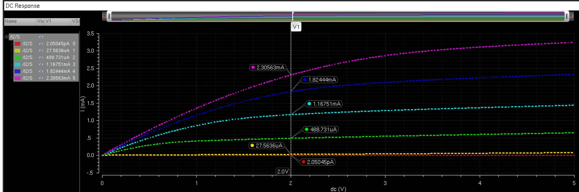
Each
of the different curves represent different values of VGS being
simulated with our sweeped Drain voltage source. As VGS increases in
voltage,
we can see that the maximum current Id also increases in a sqrt shape curve.

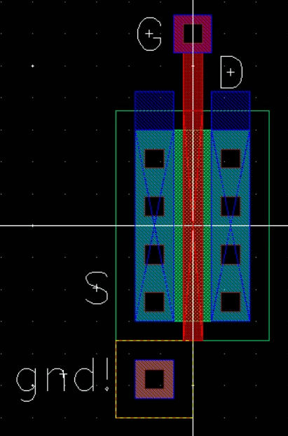
For our layout, we will use the components of m1_poly, nmos, and ptap.
We set our width to the 6u and length to 600n to our nmos component.
Our instance of m1_poly will be connected to our poly to our nmos.
The ptap will be adjacent to our nmos component.
The ptap is our bulk, or in this case, our ground. Either sides of the
nmos component will be the source and drain (it doesn't matter which)
And the connection from metal1 to our poly layer will be our gate.
We can extract our layout and compare it to our schematic. They should match!

PMOS Transistor:
Below is the schematic and symbol for the PMOS. We connect the pmos4
instance to our inputoutput pins of
Gate, Source, Drain, and Bulk. Notice that for the PMOS, the current will be going from our Source to our Drain, the opposite of the NMOS.


We have our symbol and our PMOS transistor ready to use, we can go
ahead and put it in another schematic for the purpose of simulating.
We can connect our gate to a variable voltage Vdd - VSG. In other words, as VGS approaches the value of Vdd, our PMOS
will "turn on" more and more until the max of VSG = Vdd.
Like the NMOS, we can set our variable voltage VSG to 0. We will be doing a dc sweep of our V1/VSD
or the voltage going
to the drain. It will go from 0 to 5V in steps of 1mV.
Our output will be the current going through the input of our PMOS, node S.
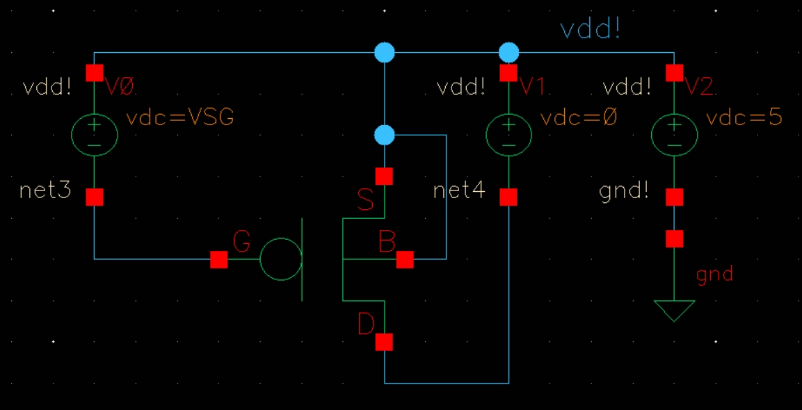

Once again, we use the parametric analysis to allow our VSG to sweep from 0 to 5V.

We will get the simulation below after pressing simulation button.
Each
of the different curves represent different values of VSG being
simulated with our sweeped Vsd voltage source.
As VSG increases in
voltage, we can see that the maximum current Is also increases in a similar shape to our NMOS Id.
Note that because our VSG is increasing, that means that the voltage going to our PMOS Gate is actually approaching 0V.
In other words, the PMOS "turns on" when the gate voltage is 0V and the NMOS "turns on" when the gate voltage is Vdd.

For our layout, we will use the components of m1_poly, pmos, and ntap.
We set our width to the 12u and length to 600n to our nmos component.
Our instance of m1_poly will be connected to our poly of the pmos.
The ntap will be adjacent to our pmos component.
The ntap is our bulk, which is usually connected to Vdd. Either sides of the
pmos component will be the source and drain (and again, it doesn't matter which)
And the connection from metal1 to our poly layer will be our gate.
The PMOS looks a bit thicker because we are using a
P-substrate so we have to implant an n-well to create our PMOS.
We can extract our layout and compare it to our schematic. They should match!

Lab Work:
Generate 4
schematics and simulations (see the examples in the Ch6_IC61 library, but note that for the PMOS body should be at vdd! instead of gnd!):
For this section of the lab, we will be looking at the schematics made in the prelab and modify them.
- A
schematic for simulating ID v. VDS of an NMOS device for VGS varying from
0 to 5 V in 1 V steps while VDS varies from 0 to 5 V in 1 mV steps. Use a 6u/600n width-to-length ratio.


We get the results that we expect. With an increasing VGS (each individual curve), our Id goes up with respect to VDS.
- A
schematic for simulating ID v. VGS of an NMOS device for VDS = 100 mV
where VGS varies from 0 to 2 V in 1 mV steps. Again use a 6u/600n width-to-length ratio.


We get the results that we expect. With an increasing VGS, our Id goes up as well.
- A
schematic for simulating ID v. VSD (note VSD not VDS) of a PMOS device
for VSG (not VGS) varying from 0 to 5 V in 1 V steps while VSD varies
from 0 to 5 V in 1 mV steps. Use a
12u/600n width-to-length ratio.


We
get the results that we expect. With an increasing VSG (each individual
curve/ a decreasing Gate voltage), our Id goes up with respect to VSD.
- A
schematic for simulating ID v. VSG of a PMOS device for VSD = 100 mV
where VSG varies from 0 to 2 V in 1 mV steps. Again, use a 12u/600n width-to-length ratio.


We get the results that we expect. With an increasing VGS, our Id goes up as well, however, it should be noted that
the threshold voltage is higher. This is because the mobility of electrons is half of the NMOS.
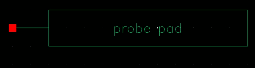
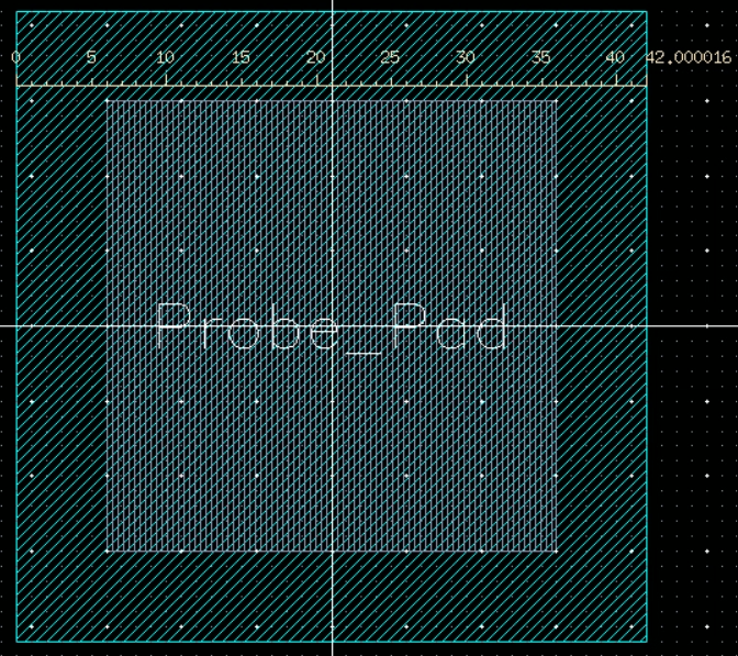
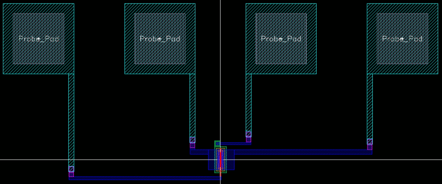
For the next section of our lab, we will require probe pads. In a schematic, they will be an input pin and on the layout,
they will be similar to a bonding pad (Metal3 with smaller glass).

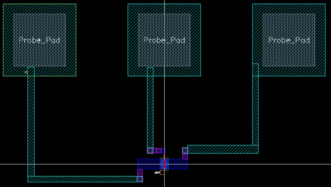
- Lay out a
6u/0.6u NMOS device and connect all 4 MOSFET terminals to probe pads
(which can be considerably smaller than bond pads [see MOSIS design rules]
and directly adjacent to the MOSFET (so the layout is relative small).
The layout will be similar to our prelab, but simply connect probe pads
at each pin.
- Show your layout passes DRCs.
- Make a corresponding schematic so you
can LVS your layout.


- Lay out a
12u/0.6u PMOS device and connect all 4 MOSFET terminals to probe
pads.
- Show your layout passes DRCs.
- Make a corresponding schematic so
you can LVS your layout.


Return to my labs
Return to student labs