Lab Project - ECE
421L
Authored by David Pinales,
Today's date: 11/6/21
Email: pinales@unlv.nevada.edu
Lab description: design a register file (RF) that uses an 8-bit
word and has 32 words. The RF uses a 5-bit address to access the 32 8-bit
words. Other inputs to the RF are the 8-IO lines for reading and writing, a
control signal, RW, for indicating either a read or write to the RF, and
VDD/ground.
Introduction:
The increasing
proliferation of battery-powered gadgets in recent years has made low power
memory design a need in the business. As the number of transistors rises, the
leakage current increases, making the SRAM unit a power demanding block from
both a static and dynamic standpoint. Nowadays, the SRAM block is also a key
aspect of SOC architecture. The key concerns in developing the memory are power
dissipation and area. Memory density scaling must continue to match logic
scaling advances in memory design.
Components of SRAM:
The main SRAM building blocks include various
components. All these components or blocks used in the SRAM are listed as
follows:
• SRAM cell • Pre-Charge Circuit • Write Driver
circuit • Sense Amplifier • Address decoder
6-Transistor SRAM Single Cell:
Description:
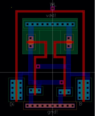
The 6 Transistor SRAM Cell is a component in
which operates for low voltage, low power behaviors. This component uses a
bistable latches system in which tells the circuitry on how to handle the bits
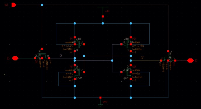
coming in. M1 and M2 PMOS are the pull up transistors whereas M3 and M4 NMOS
are the driver transistors. Access is provided through a word line (WL) that
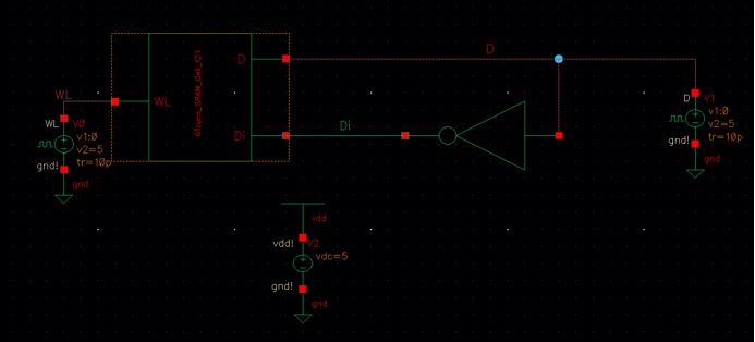
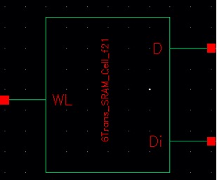
connects to M5 and M6 pass transistors, resulting in Di and D (Data) lines that
are utilized for both reading and writing. These bit lines help to increase the
noise margin. Differential circuitry allows for noticeable output voltage
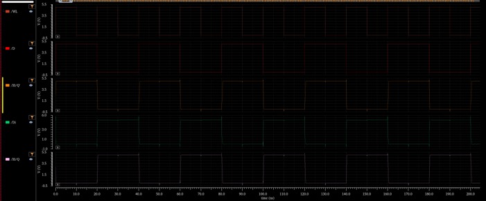
fluctuations. It stores logic 0 or 1 if the power is turned on, therefore
unlike DRAM cells, it does not need to be updated. The size of the transistors
in SRAM architecture is critical to its proper operation. Beginning with
inverters, the width of the NMOS is 1.5um, and because the NMOS is
almost twice as conductive as the PMOS, W=1.5um is used to balance their
conductivity. The gateway transistors, on the other hand, must be 2 or 3 times
bigger than the NMOS transistors from the inverters to be conductive enough to
modify the logic level held by these transistors. However, they should not be
too enormous so that they take up too much room. For these gateway transistors,
I chose a width of 6um.
Schematic:
Simulation:
Holds
Symbol:
Layout:
The write driver is responsible for swiftly
discharging the bit lines to a level underneath the cell's write margin before
or while the word lines of the selected cell are active. Which bit line is
discharged is determined by the data supplied. Only when a writing operation is
intended is the WL signal activated. Otherwise, the WL separate the bit lines
from the write drivers. It is quicker because it has fewer stacked transistors
in its discharge route, but it is more complicated. Typically, the writer of
the operation is not a time-critical transaction, simpler configurations that
loosen the layout constraints are recommended for the write driver. It is made
up of CMOS inverters and NMOS pass transistors and may be scaled up since the
number of transistors required to construct a column is not dependent on the
number of transistors.
8-Bit Memory Word Cell:
Description:
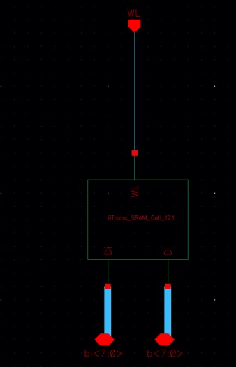
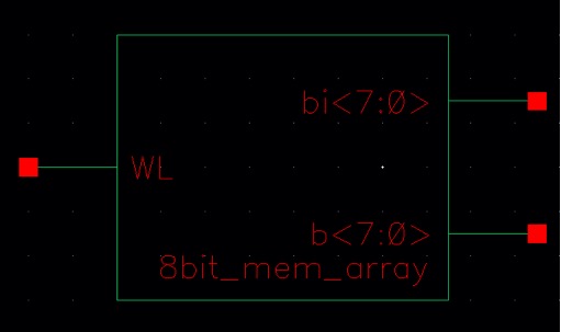
Here we are combining our Single 6T component
into a 8-Bit memory word cell.
Schematic:
Symbol:
Simulation:
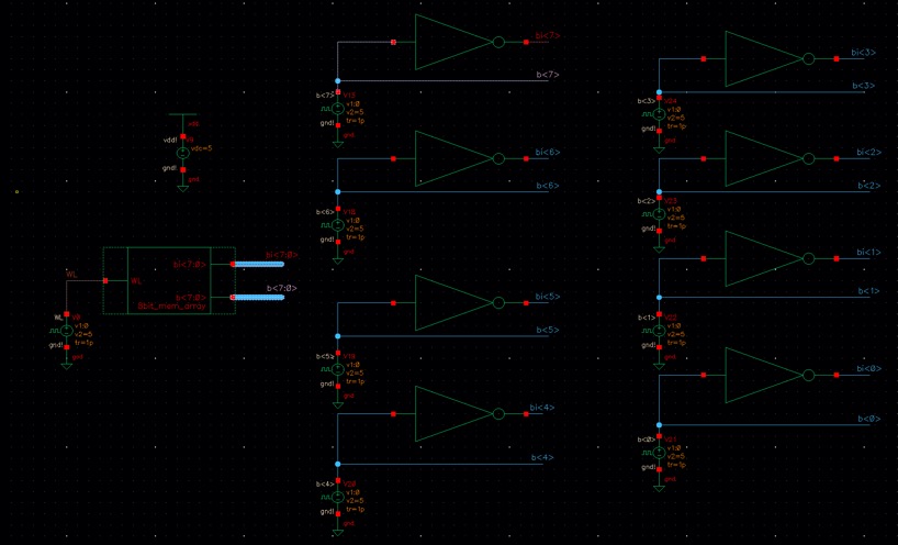
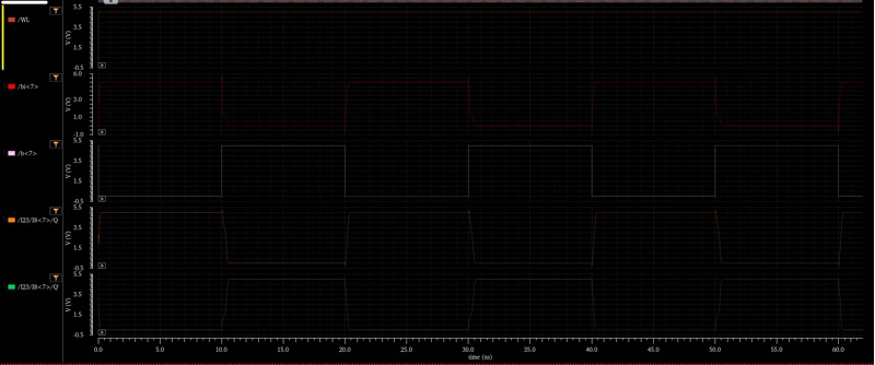
With WL enabled to HIGH, We
can see the bit are Holding well.
Layout for 8bit memory single cell:


8-Bit Word Array:
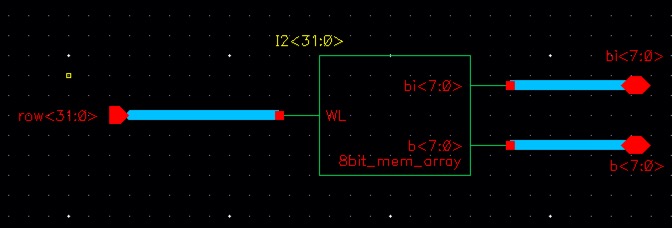
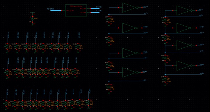
Schematic for 8bit word array (32*):
Simulation:
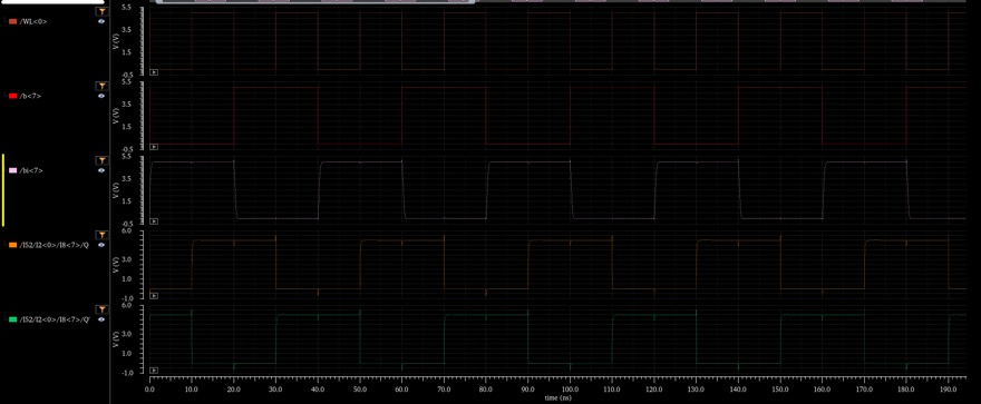
As we descend into Bit<7>, Row<0>,
We can see how the push through given components are holding well with both
operations so Write and read are displayed
![]()
![]()
![]()
![]()
![]()
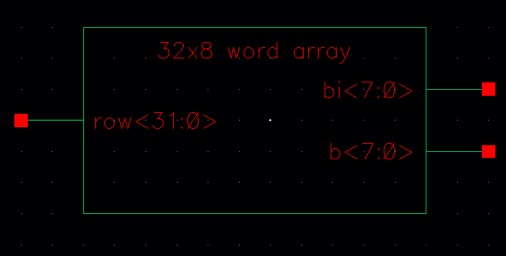
Symbol For 32x8 Word Array:
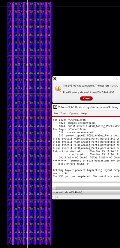
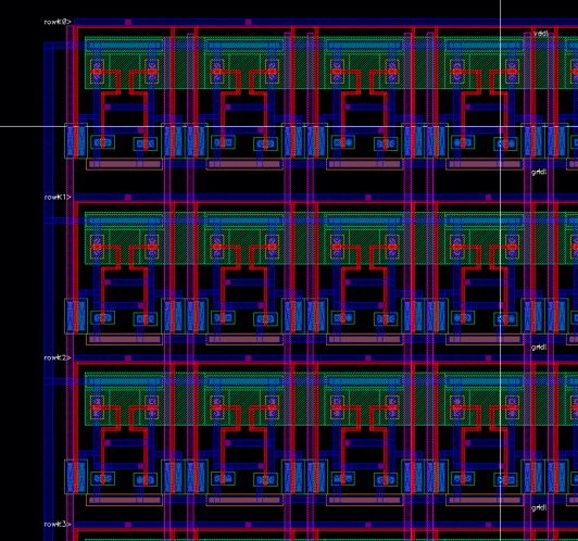
Layout:
Address (5:32) Decoder:
Description:
Multiple words are put in one row in programs
that use the standard word size (M<128). Interleaved bits of words in a row
share peripheral circuitry such as a sense amplifier, write driver, and row
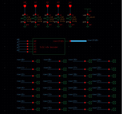
decoder. In this case, an address decoder is utilized to decode the input
address and enable the word line. 7 dynamic NAND CMOS decoders are employed
here. One is employed as a row decoder, which picks a certain word line by
increasing its voltage level. The column decoder determines which column to
use. In this case, a 5:32 NAND CMOS decoder is employed, with an inverter added
to access it during the write phase. As the project details ask for a
5-to-32-bit decoder.
Schematic (5:32 Row Decoder):

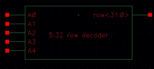
Symbol:
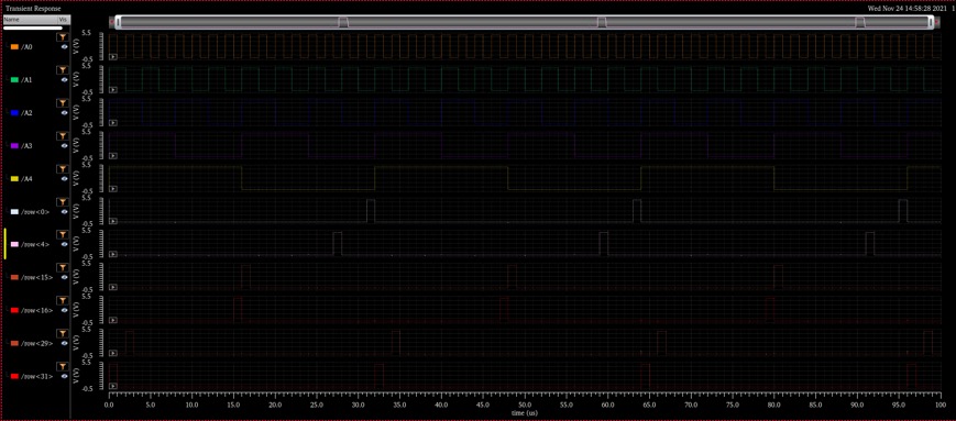
Simulation:
Here can be seen gathering different parameters
from individual rows. I chose the given rows to show the variety of Behaviors
occurring.
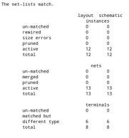
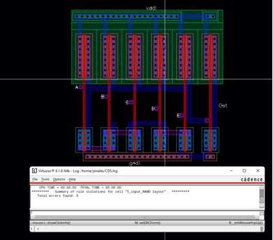
Layout - 5 Input-NAND:
Layout of 5:32 Decoder:
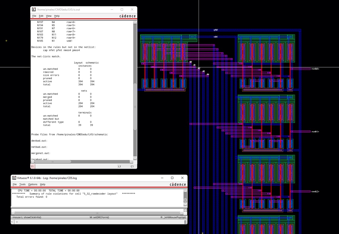
32 bit-word
SRAM Register File:
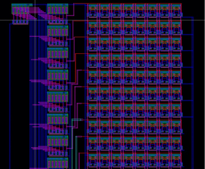
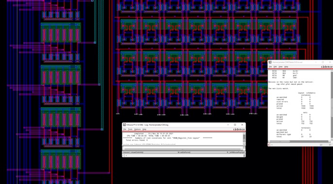
Description:
For the result,
I have combined my 5:32 Decoder into the 32:8 Bit word array to finalize my
32-Bit SRAM Register File.
Schematic/ Simulation:

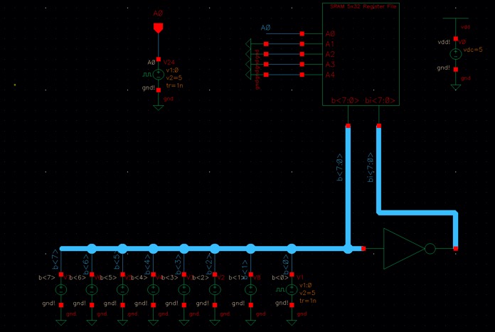
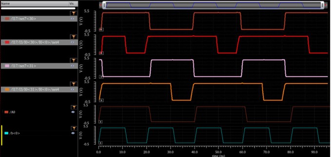
*As you've seen, the registration file is
operational.
We set
the specific address of "00001" when A0 is high, which writes to
row<30>. This causes I0<30> to follow b<0>.
When A0 is low, the address "00000" is
called, and we are writing to RL31>, thus I0<31> now comes after
b<0>*
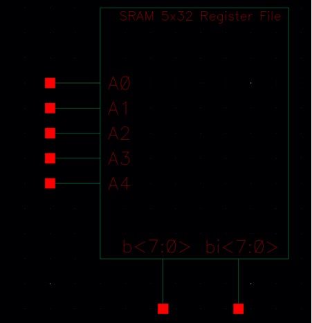
Symbol:
Layout:
![]()
![]()
![]()
![]()

![]()
****Added Features that assist for Static Noise
Margin****
Pre-charger:
Description:
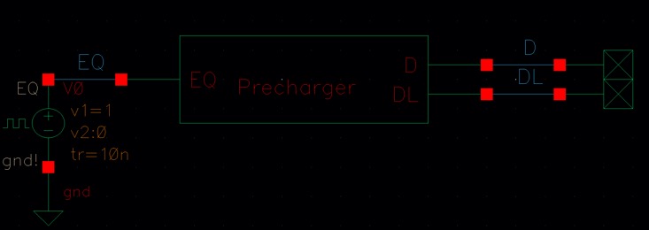
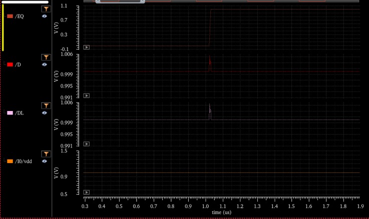
The pre-charge of the bit lines is critical to
the proper operation of the SRAM. To accomplish the read operation, the bit
lines must be charged at the same voltage. Following the writing and reading
operations, one of the bit lines is drained, resulting in an unwanted voltage
differential between the bit lines. Following these procedures, the pre-charge
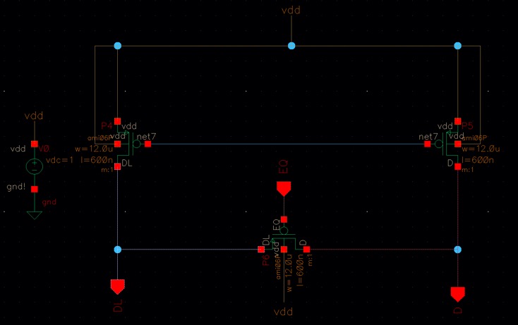
circuit equalizes the bit line voltages to the supply voltage. M1 and M2 PMOS
transistors will precharge the operation, and M3 PMOS
transistor will equalize the operation when Vdd is
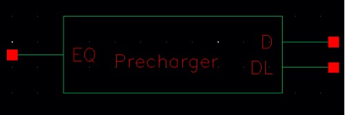
presented in this input. My schematic below depicts the circuit diagram of the precharge circuitry, and Vdd=1v
is used.
Schematic:
Simulation:
Symbol:
Sense
Amplifier:
Description:
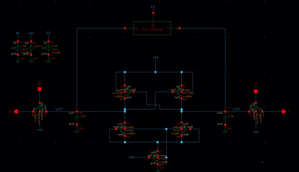
A modest
analog differential voltage is created on the bit lines during a read access is
amplified by the sensing amplifier. A full swing single ended digital output is
produced because of the amplification. Because the drive transistors do not
need to fully discharge the bit lines, the use of SA (Sense Amplifier)
minimizes the size of the SRAM cell. In general, read operations are the
slowest, causing a delay in the cell. Because of the length of the metal and
the number of transistors, bit lines have a higher capacitance and require more
time to discharge. The hardest choices for sense amplifiers here are time
control and load capacitor selection. The SAE signal is used for it. In this
case, a latch type sense amplifier is employed, with two cross coupled inverters
providing differential output that amplifies the signal and provides complete
swings, and two capacitors storing the level of the bit lines.
Schematic:
Conclusion
As the result still had some noise margin
induced by the component’s, the most optimal way to reduce all the noise and
contain a perfect SRAM model the additional components listed would be ideal.
With the result being as is, we still were able to obtain logic levels of 1 and
0 to induce the read or write capabilities the SRAM Register File. Furthermore,
more can be done as mentioned with the descriptions of the other components
left out, the implementation of the Pre-charger and the sense amplifier would
be ideal if another SRAM file were to be made.
Return
to other fellow 421L engineer labs