Lab 4 - ECE 421L
Created and edited by Michael Parker
Email : parkem3@unlv.nevada.edu
Last updated : September 22 2021
Pre-Lab
- Back-up all of your previous work from the lab and the course.
- Read through the lab before starting it.
- Go through tutorial 2 seen here
Lab Overview
The purpose of this lab is to show the IV characteristics of NMOS and PMOS devices and lay them out.
Lab Procedures
ID v. VDS NMOS
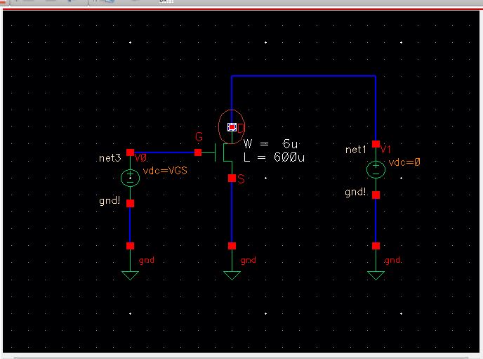
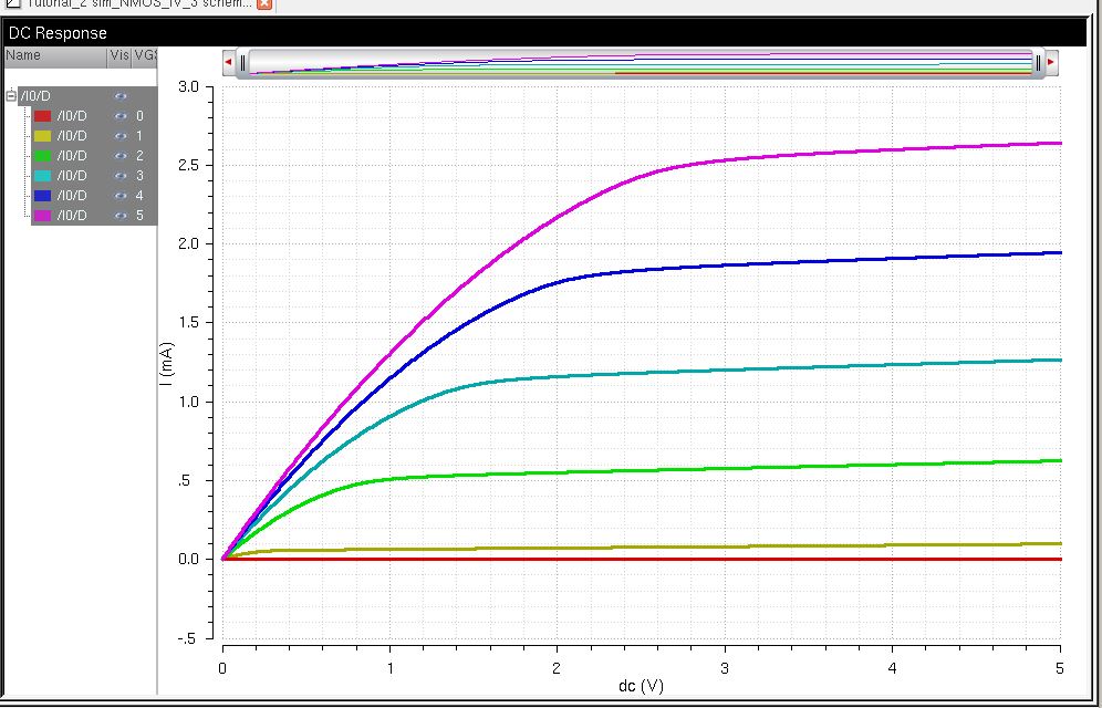
For this first task, I created a schematic and simulated ID
v. VDS of an NMOS device for VGS from 0 to 5 volts with 1 volt steps,
while varying VDS from 0 to 5 volts in 1 mV steps.


ID v. VGS NMOS
For
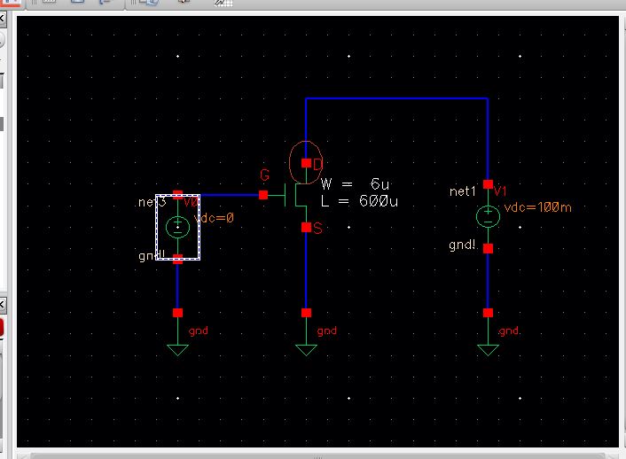
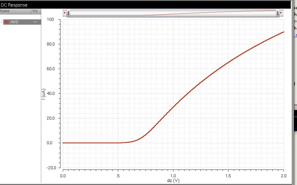
the next task, I created a schematic and simulated ID v. VGS of an
NMOS device for VGS from 0 to 2 volts with 1mV steps, while
VDS is held at 100 mV steps.


ID v. VSD PMOS
For
the following task, I created a schematic, using a 12u/600n
width-to-legnth ratio, and simulated ID v. VSD of an PMOS device
for VSG from 0 to 5 volts with 1 volt steps, while
VSD is varied from 0 to 5 volts in 1mV steps.
ID v. VSG PMOS
For
the final task of part one, I created a schematic, using a 12u/600n
width-to-legnth ratio, and simulated ID v. VSG of an PMOS device for
VSG from 0 to 2 volts with 1mV steps, while
VSD is held at 100mV.
6u/0.6u NMOS Layout
For
this task, I created a layout of a 6u/0.6u Nmos device and connected
its 4 terminals to probe pads that i placed directly adjacent to the
layout, and created a cooresponding schematic.
12u/0.6u PMOS Layout
Finally, I created a layout of a 12u/0.6u Pmos device and connected
its 4 terminals to probe pads that I placed directly adjacent to the
layout, and created a cooresponding schematic.