Lab 5 - ECE 421L
Created and edited by Michael Parker
Email : parkem3@unlv.nevada.edu
Last updated : October 5 2021
Pre-Lab
- Back-up all of your previous work from the lab and the course.
- Go through tutorial 3 seen here
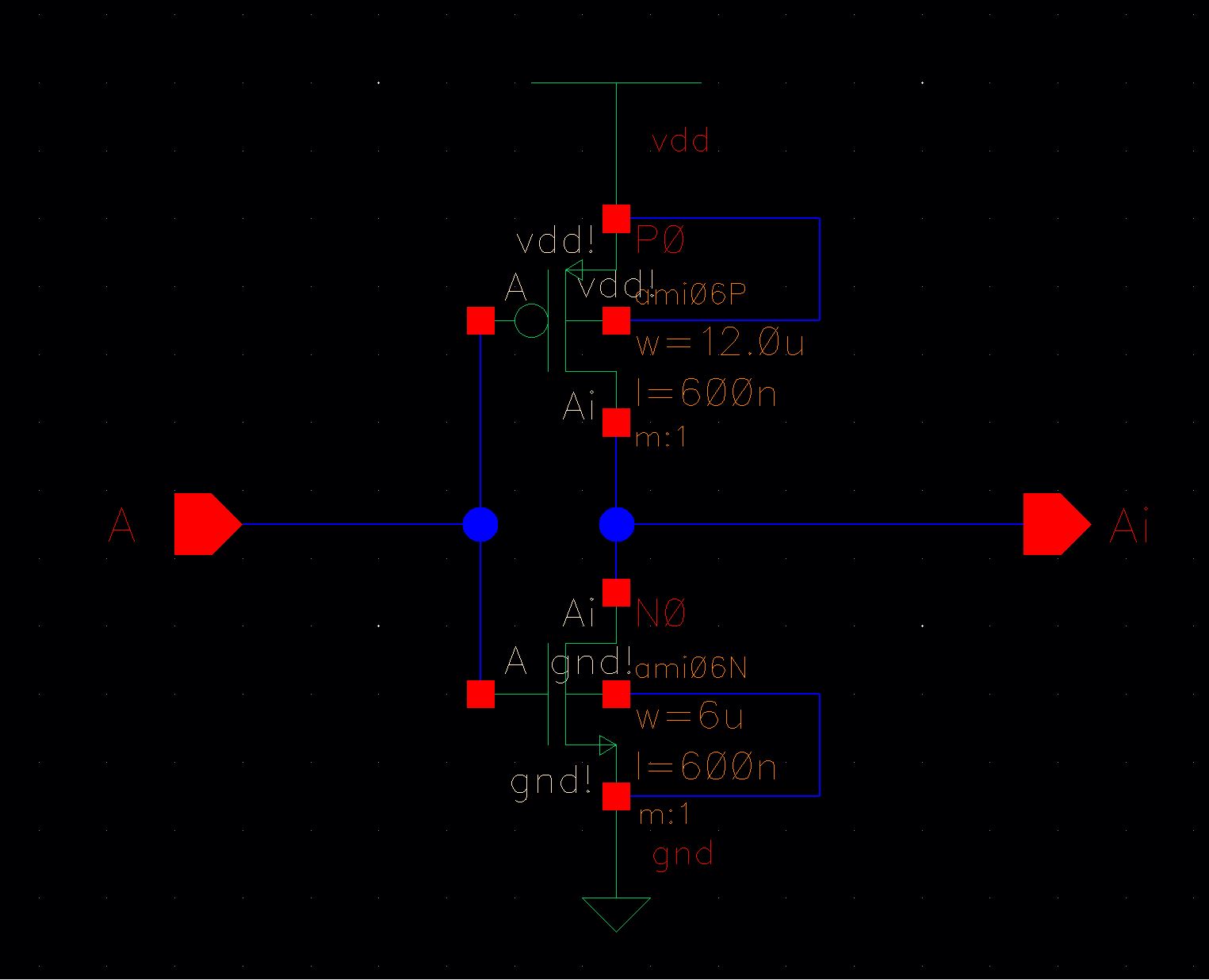
The first step was to draft a schematic of a CMOS inverter using a 4
input nmos and a 4 input pmos and create a symbol from that schematic.
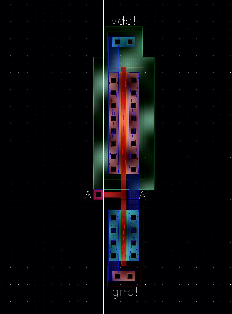
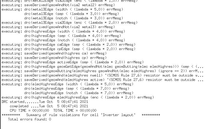
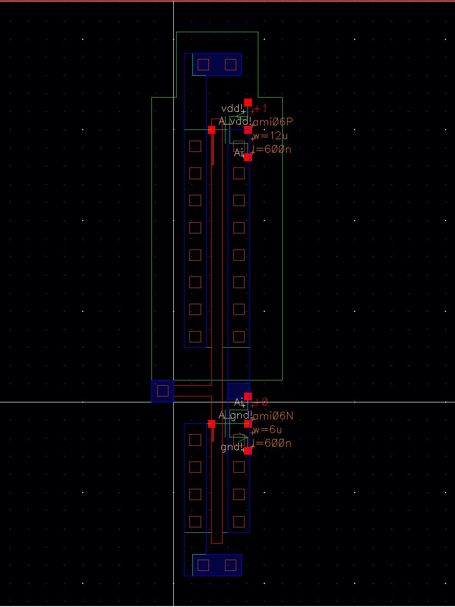
The next task was to create a layout of the inverter, DRC that layout,
extract it, and then LVS it against the schematic we drafted earlier.

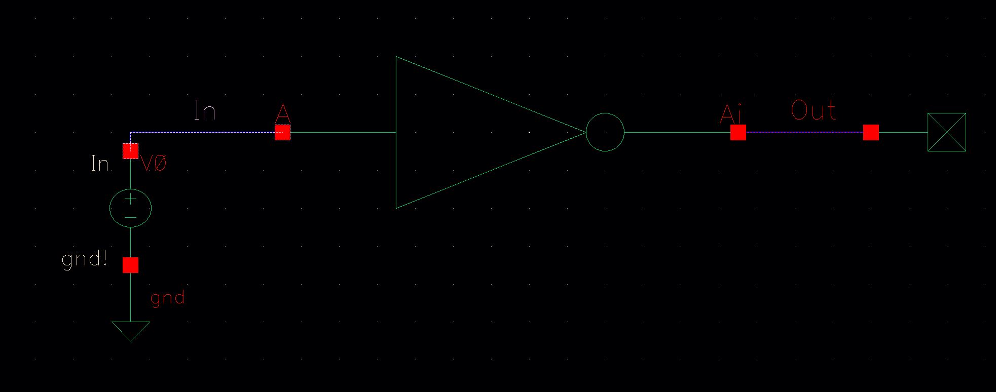
The next step was to create a schematic using out symbol to simulate
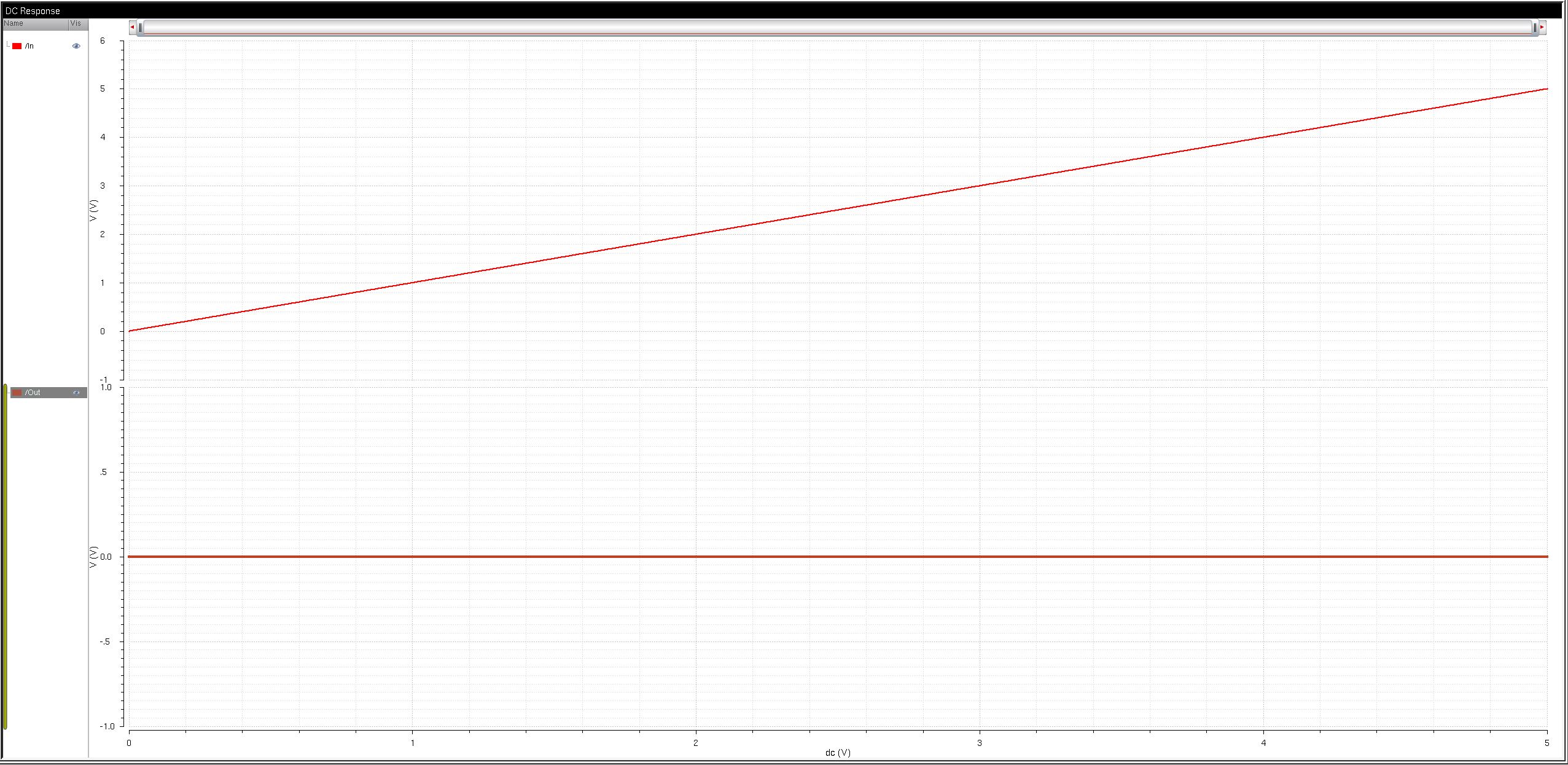
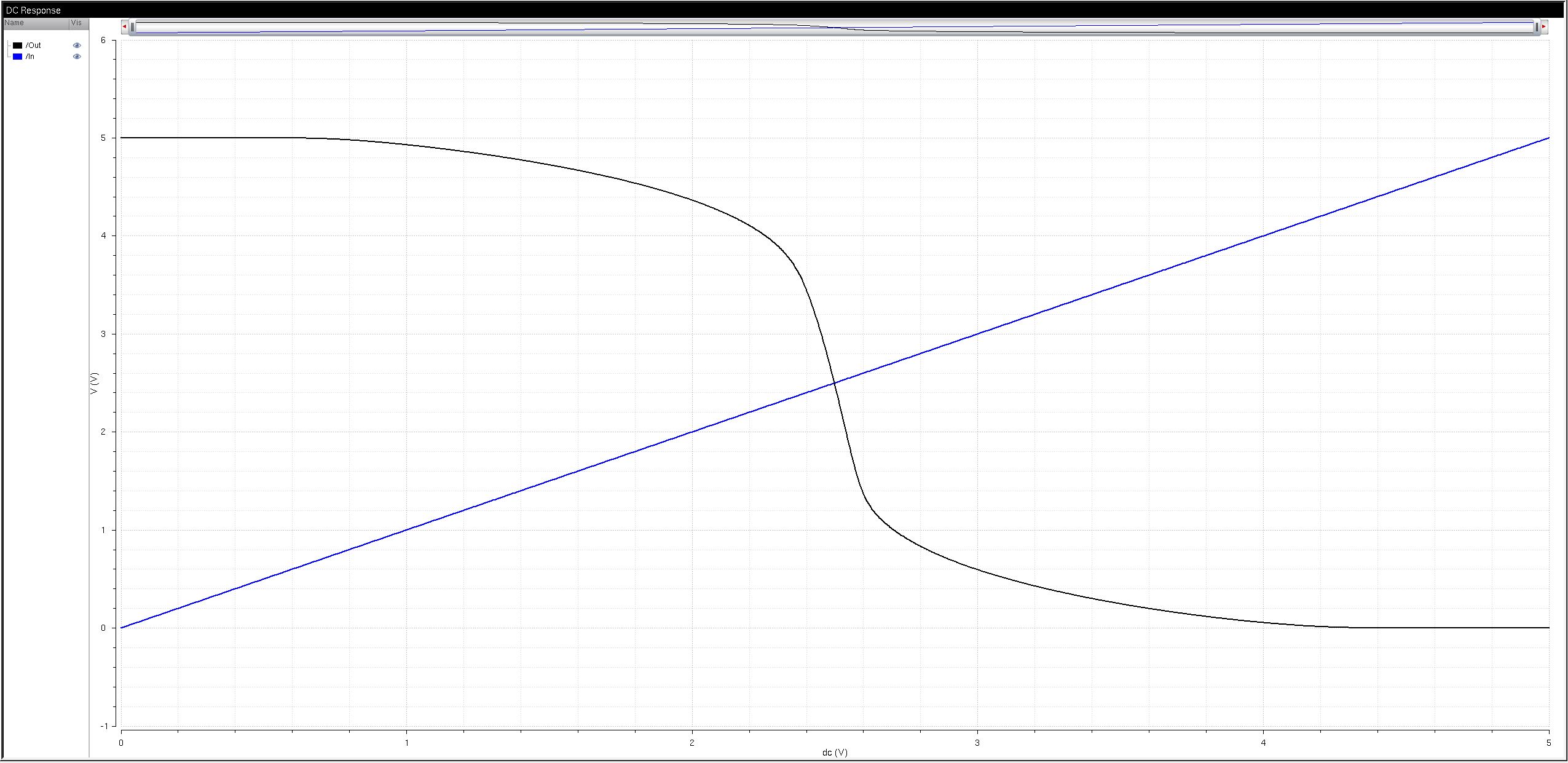
from. The output of these simulations can be seen on the strip plot and
the
plot of the voltage transfer curve.
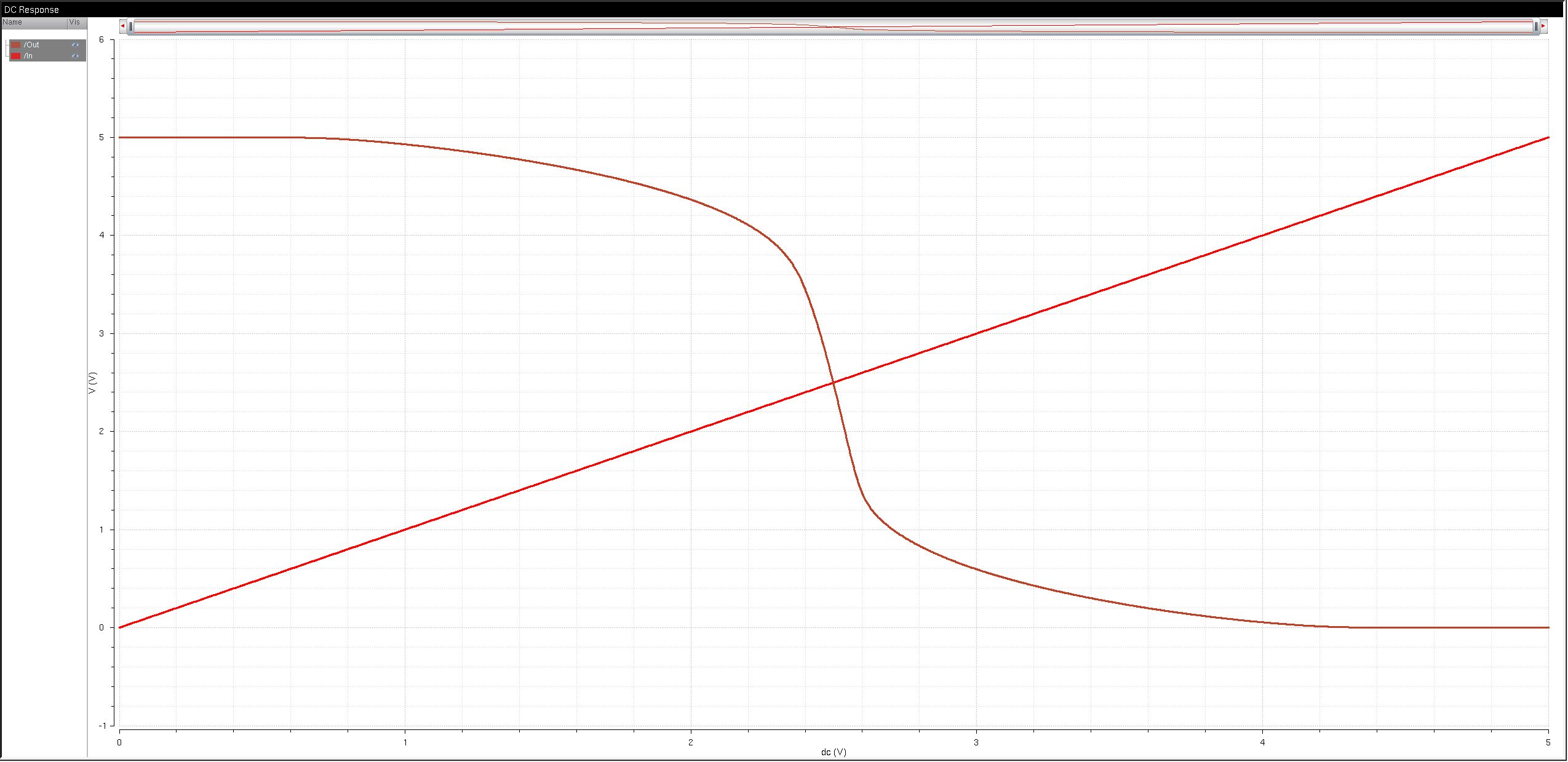
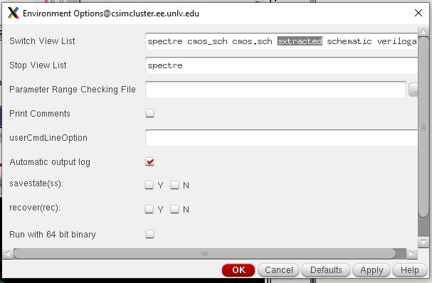
Now that we have this plot of the voltage transfer curve, we can check
it against the voltage transfer curve of our extracted layout.
Lab Overview
The purpose of this lab is to design, layout, and simulate a CMOS inverter.
Lab Procedures
12u/6u
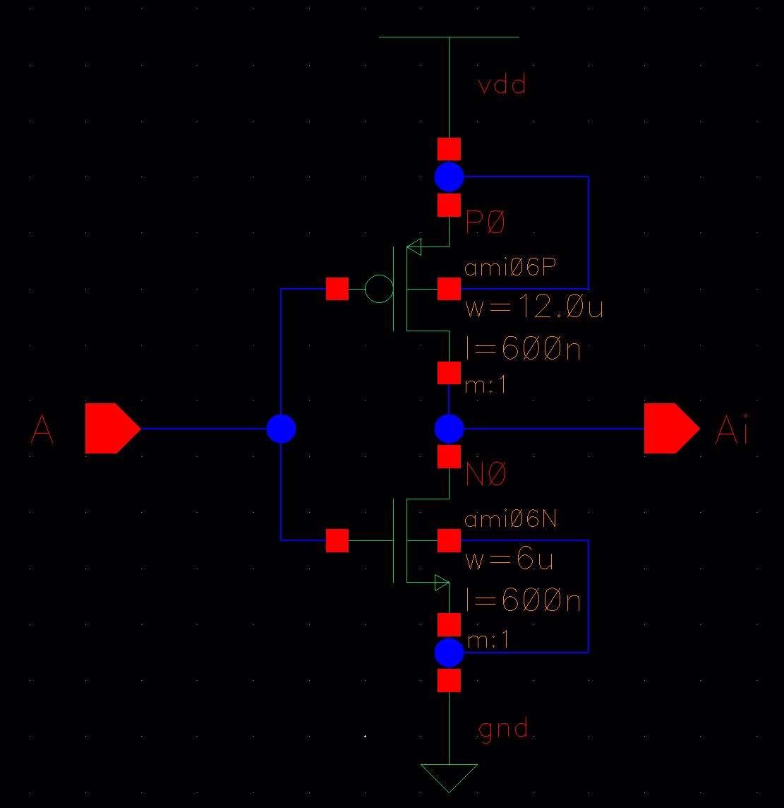
For this first task, I created a schematic of a CMOS inverter
using a width of 6um for the nmos and 12um for the pmos. Both the pmos
and the nmos
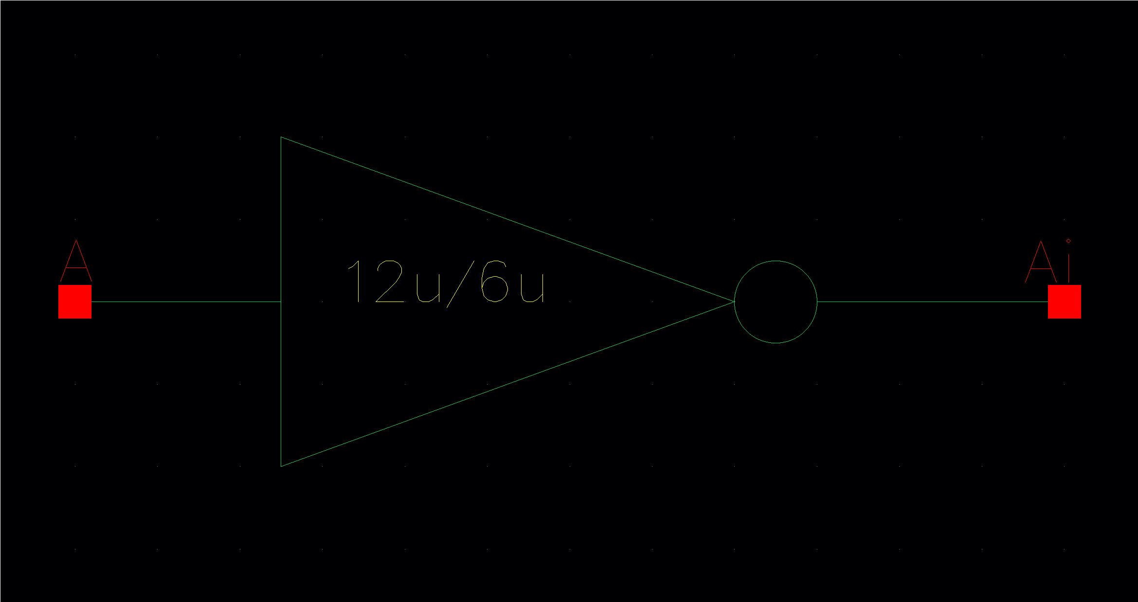
have a legnth of 600nm. I then created a symbol for the inverter I previously drafted.
Now
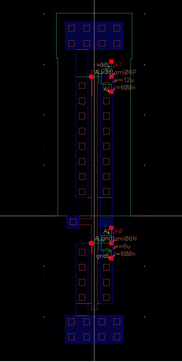
that a schematic and a symbol file were created for the inverter, I
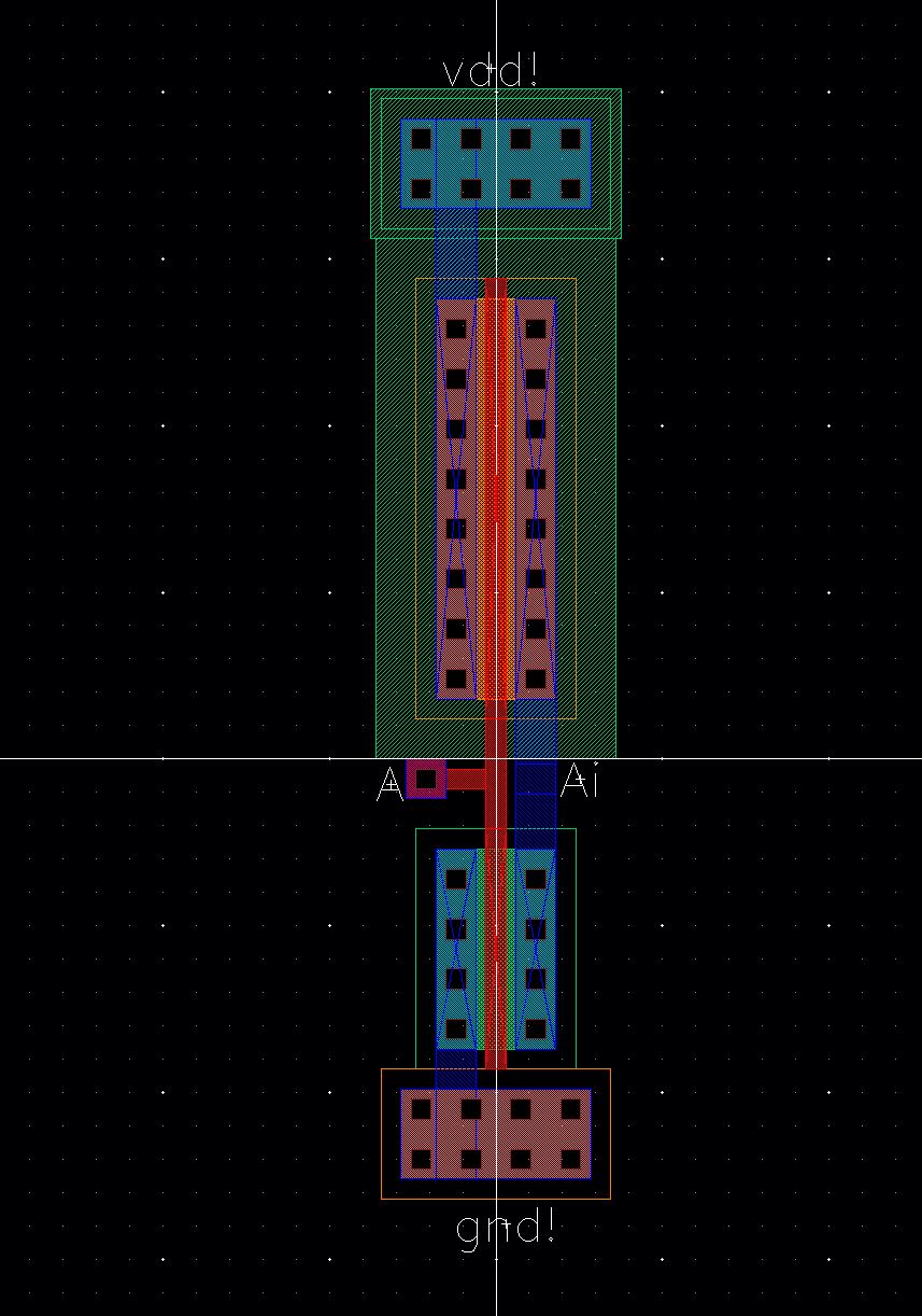
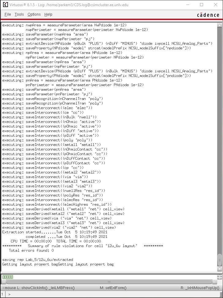
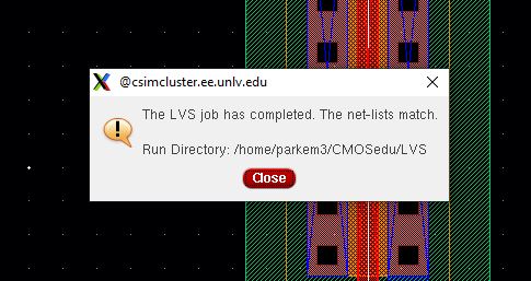
created a Layout using a single finger (or a multiplier of 1). A DRC
was run for this
Layout and its extracted view was LVSed.
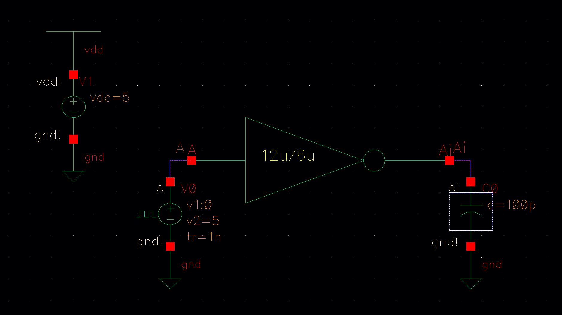
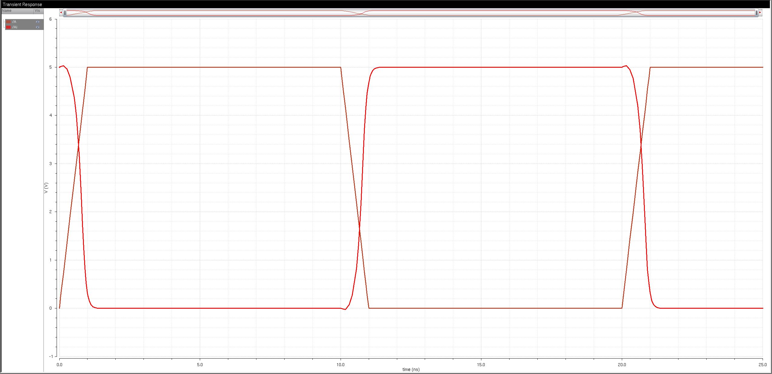
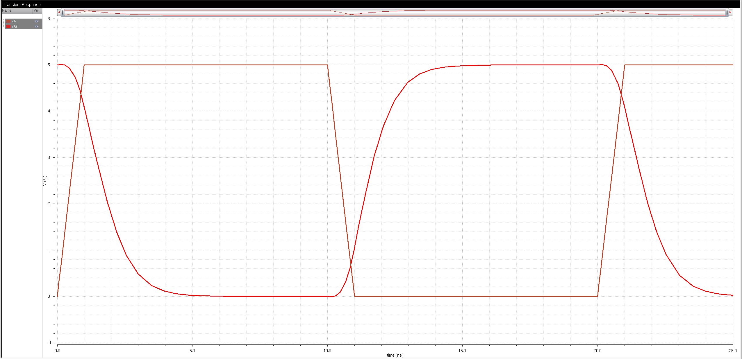
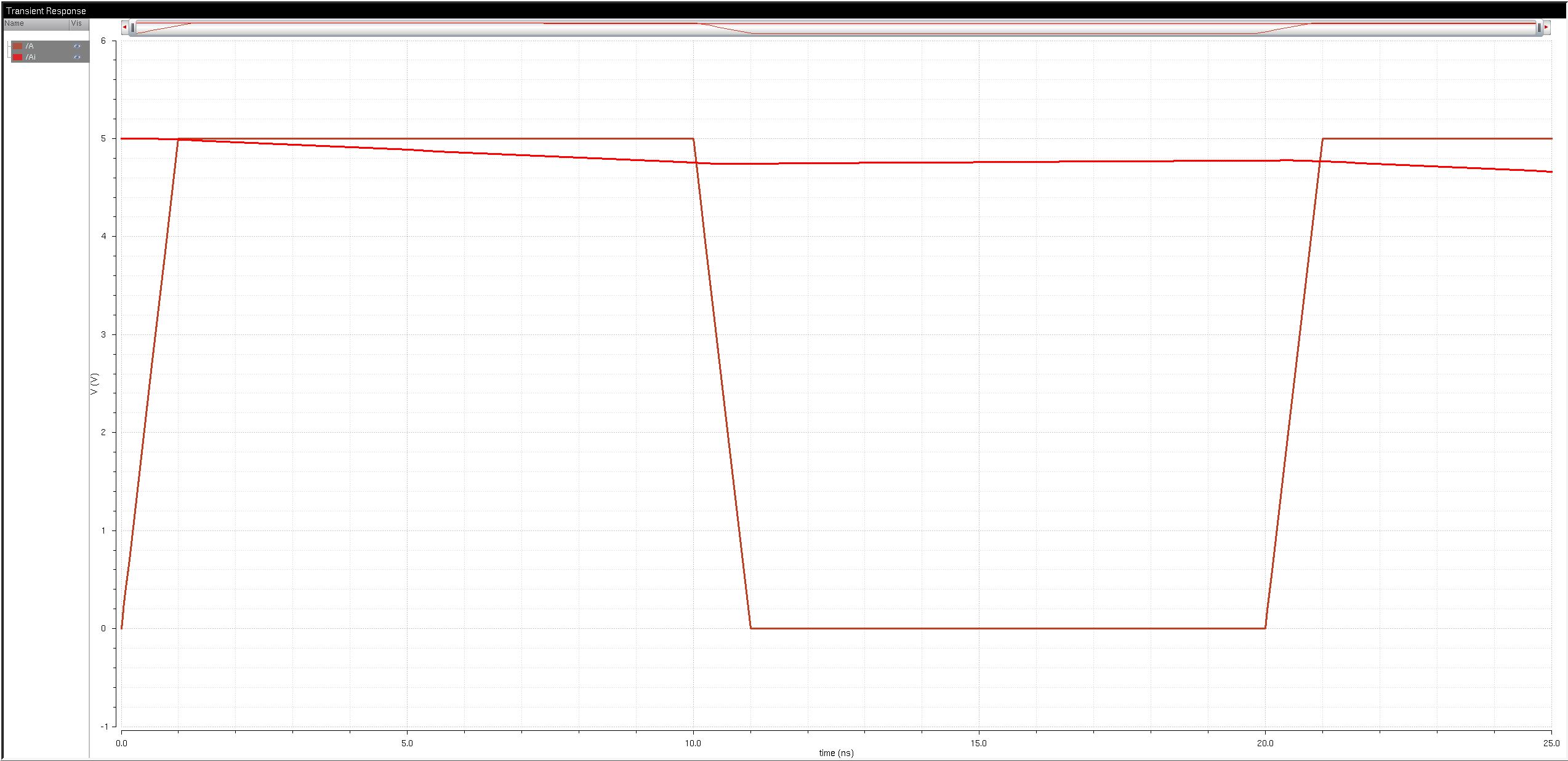
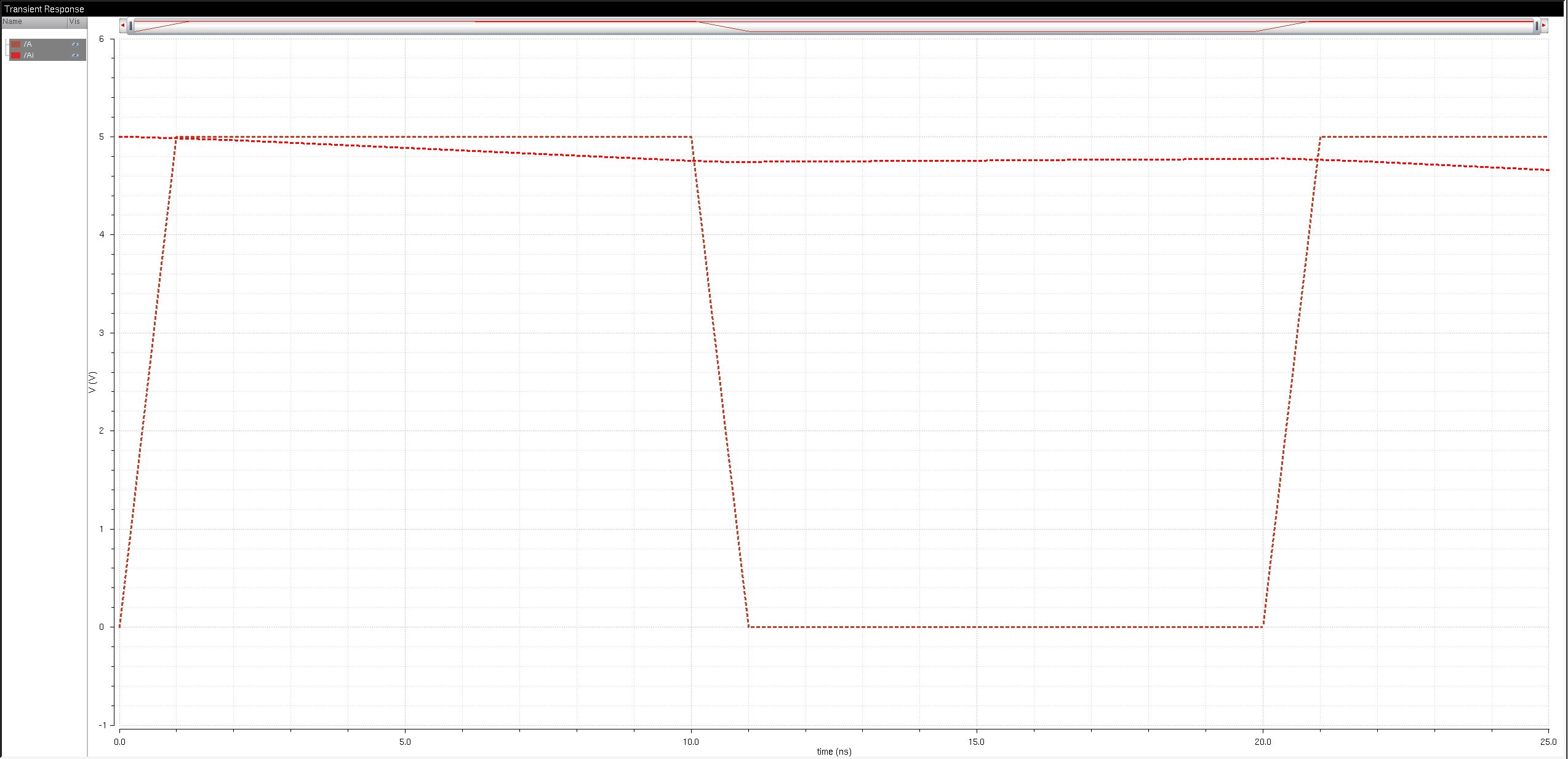
The final tasks for the 12u/6u inverter were to simulate the inverter
in a circuit driving capacitive loads of 100fF, 1pF, 10pF and
100pF using spectre. After the
spectre simulations were complete I
reran the simulations using UltraSim, showing the difference and the
accuracy sacraficed for the speed of the simulation.
| 100fF Spectre | 100fF UltraSim |

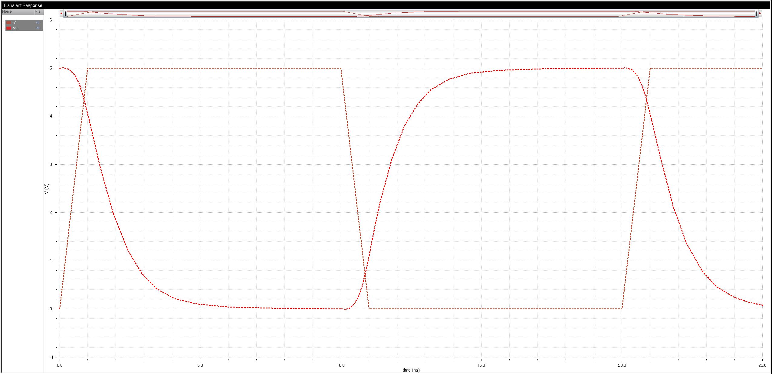
| 10pF Spectre | 10pf UltraSim |
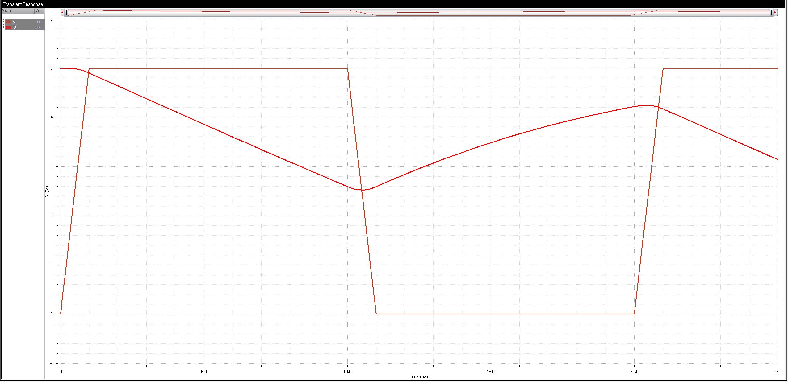
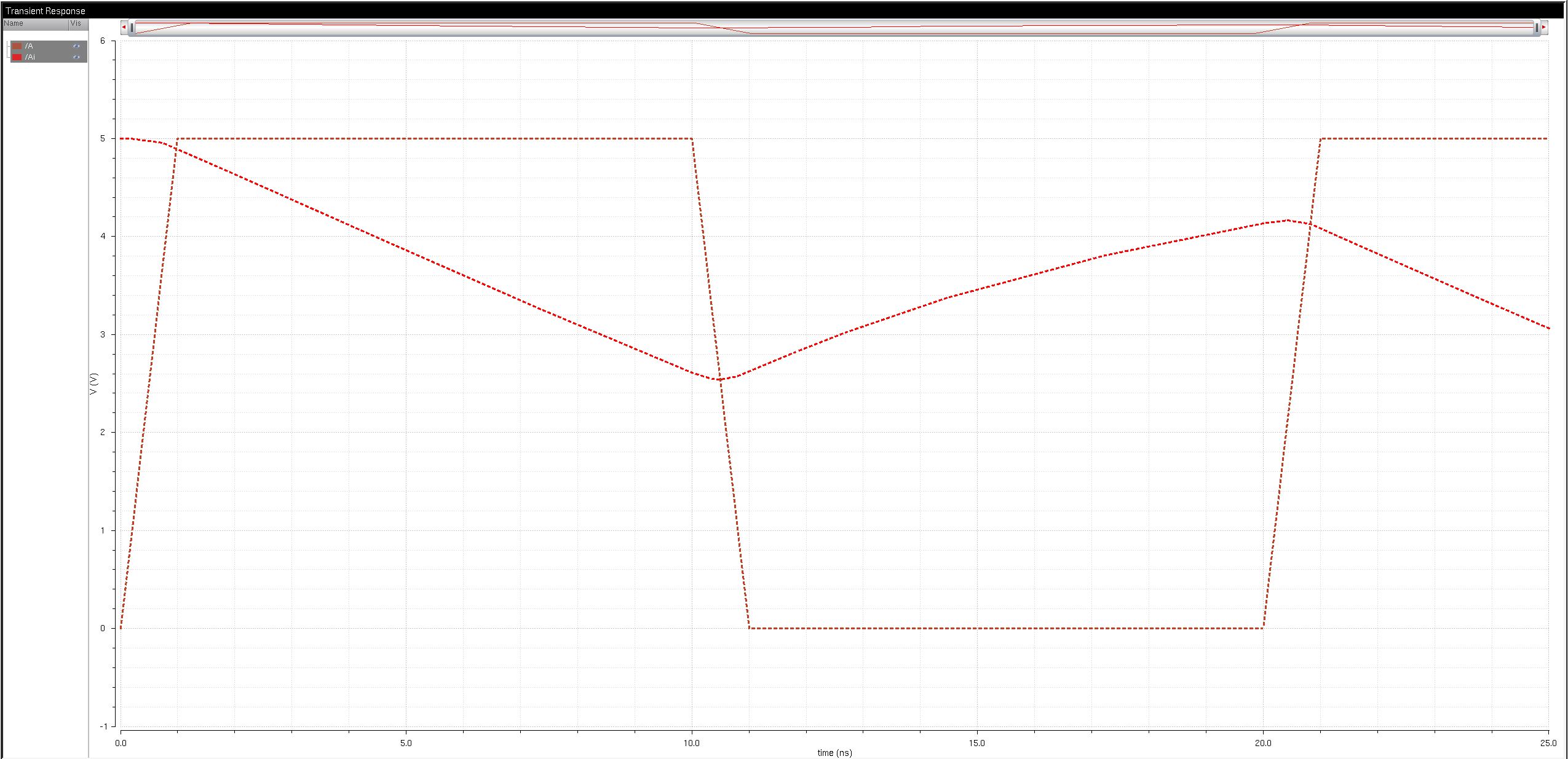
| 100pF Spectre | 100pF UltraSim |
48u/24u
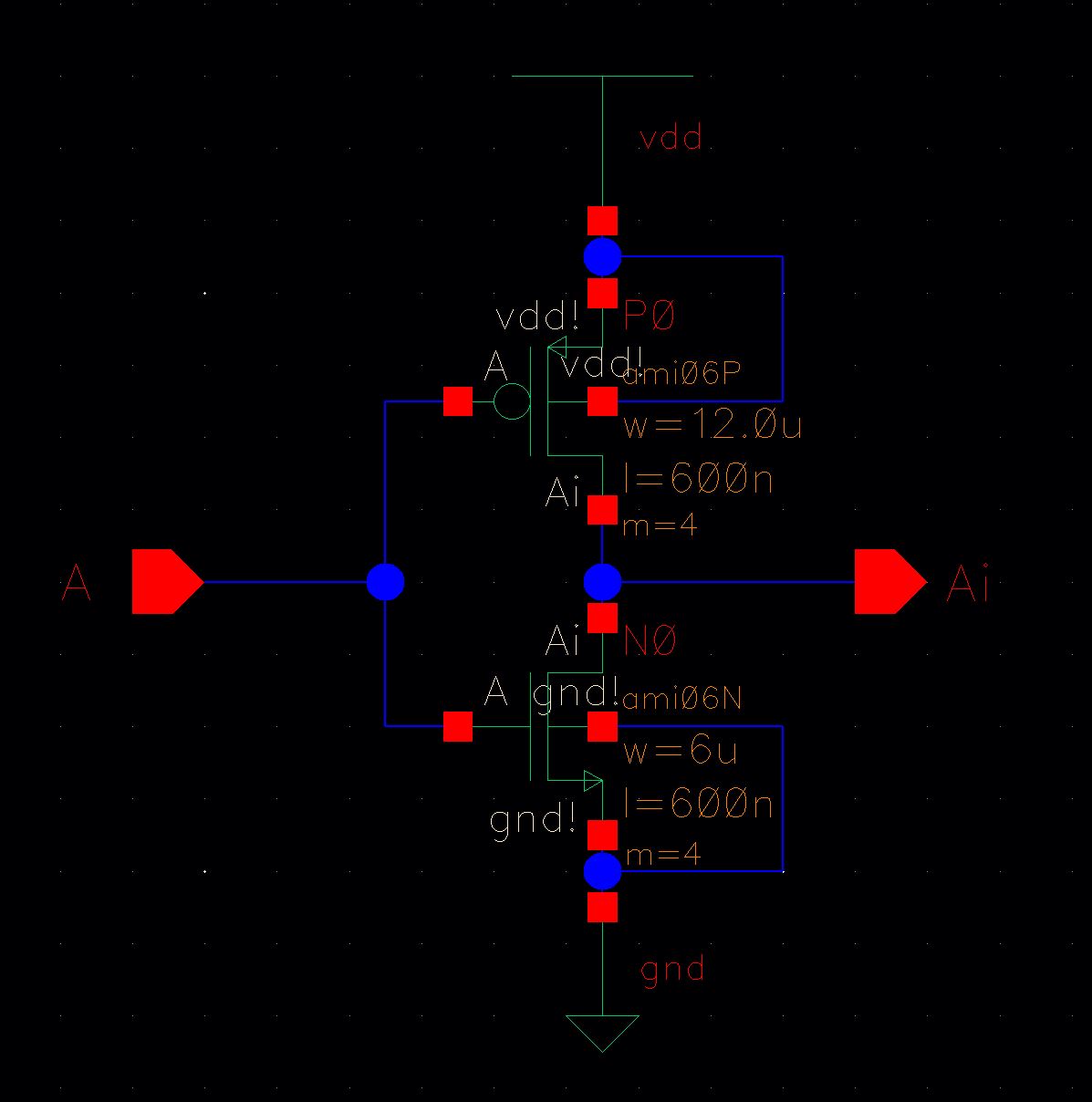
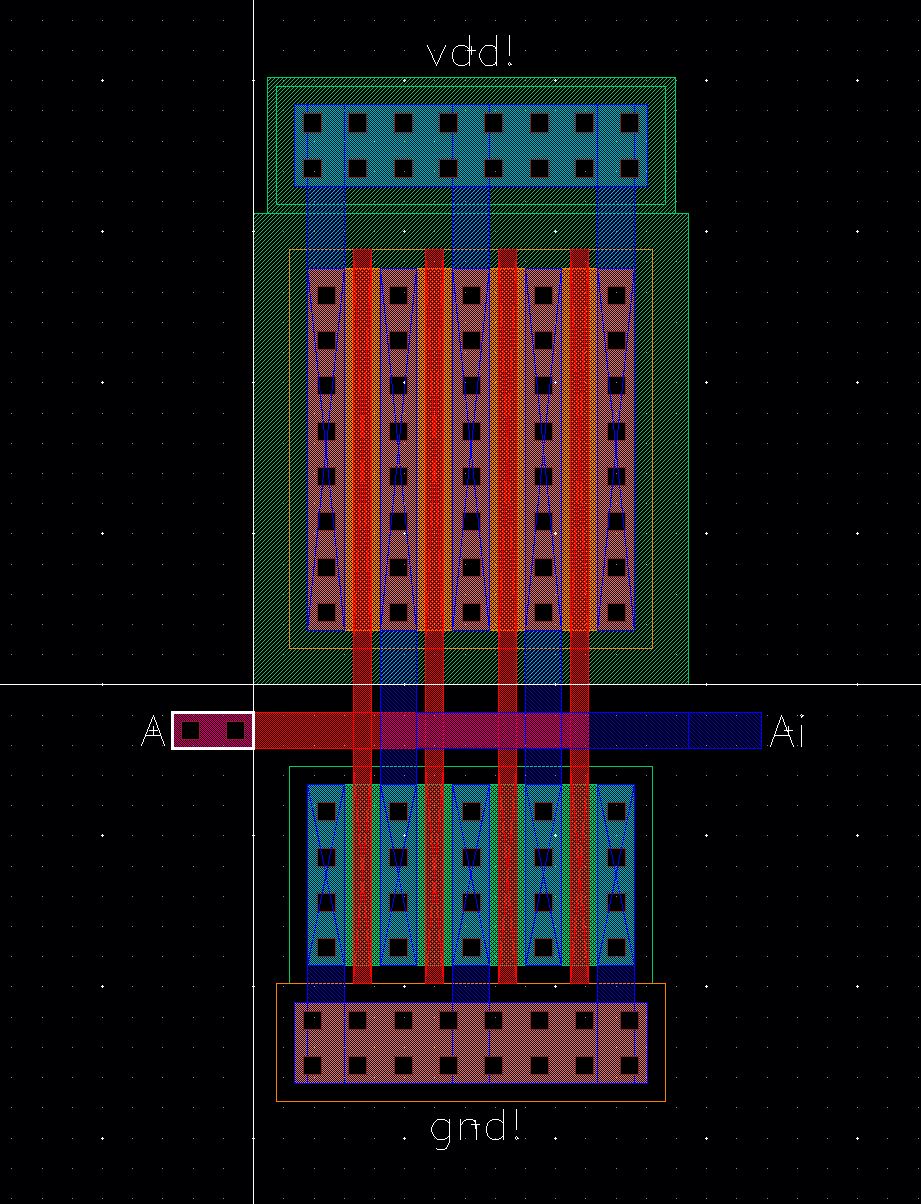
For this first task, I created a schematic of a CMOS inverter using a
width of 24um for the nmos and 48um for the pmos. Both the pmos and the
nmos
have a legnth of 600nm. I then created a symbol for the inverter I previously drafted.

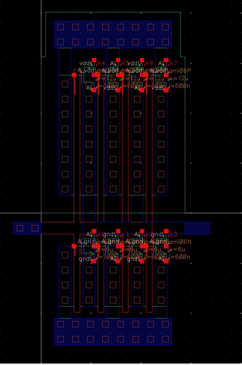
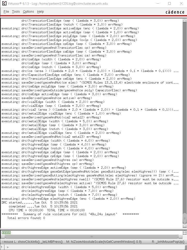
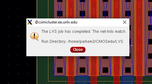
Now
that a schematic and a symbol file were created for the inverter, I
created a Layout using a single finger (or a multiplier of 1). A DRC
was run for this
Layout and its extracted view was LVSed.
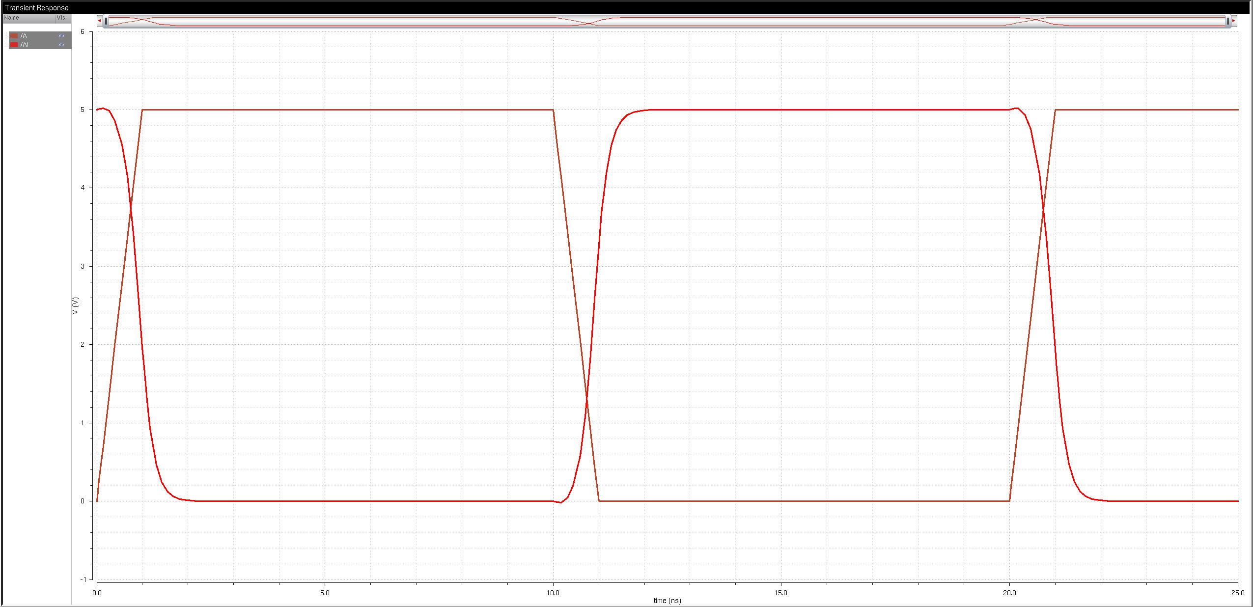
The final tasks for the 48u/24u inverter were to simulate the inverter
in a circuit driving capacitive loads of 100fF, 1pF, 10pF and 100pF
using spectre. After the
spectre simulations were complete I reran
the simulations using UltraSim, showing the difference and the accuracy
sacraficed for the speed of the simulation.
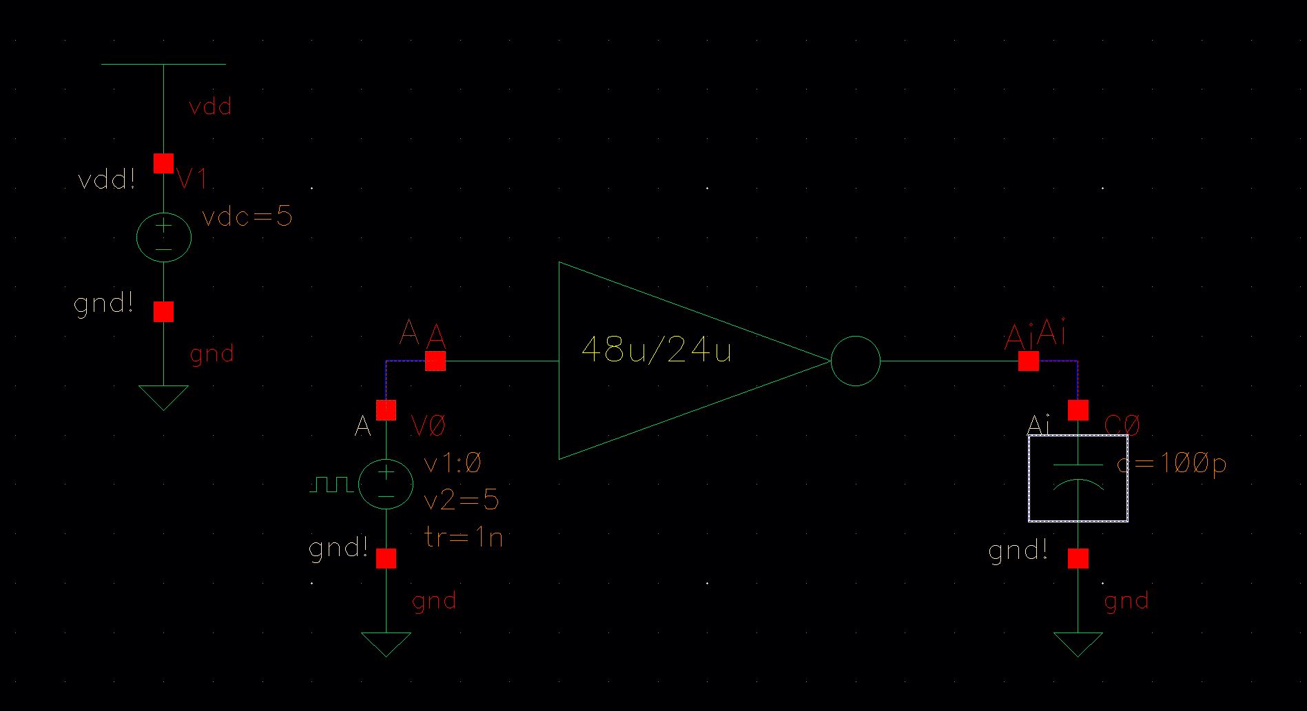
| 100fF Spectre | 100fF UltraSim |
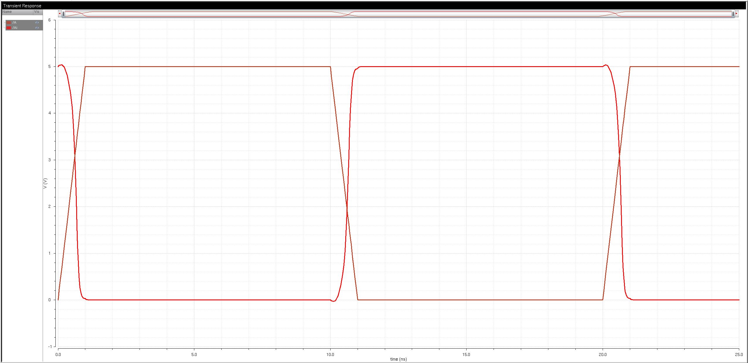
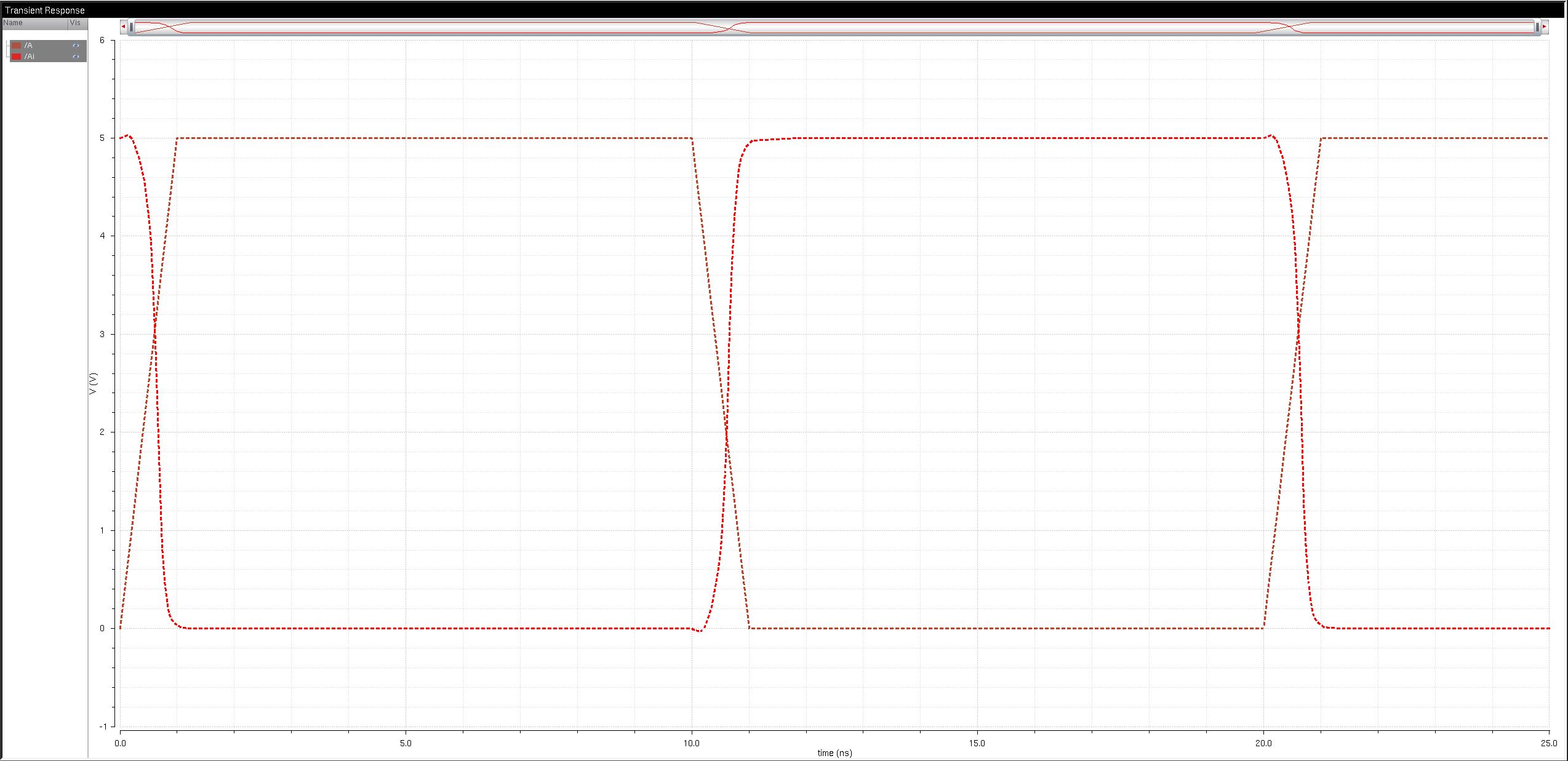

| 10pF Spectre | 10pf UltraSim |
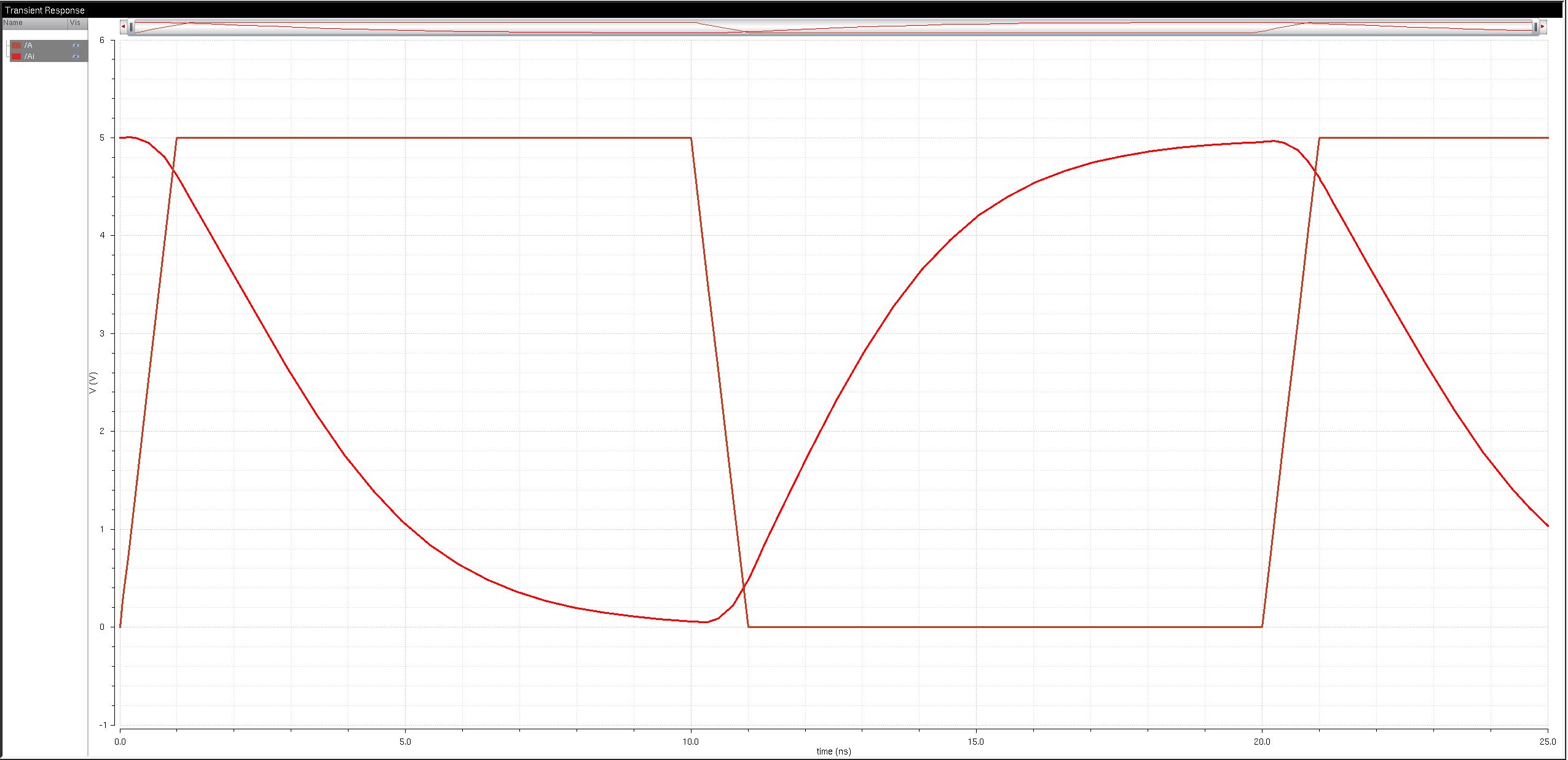
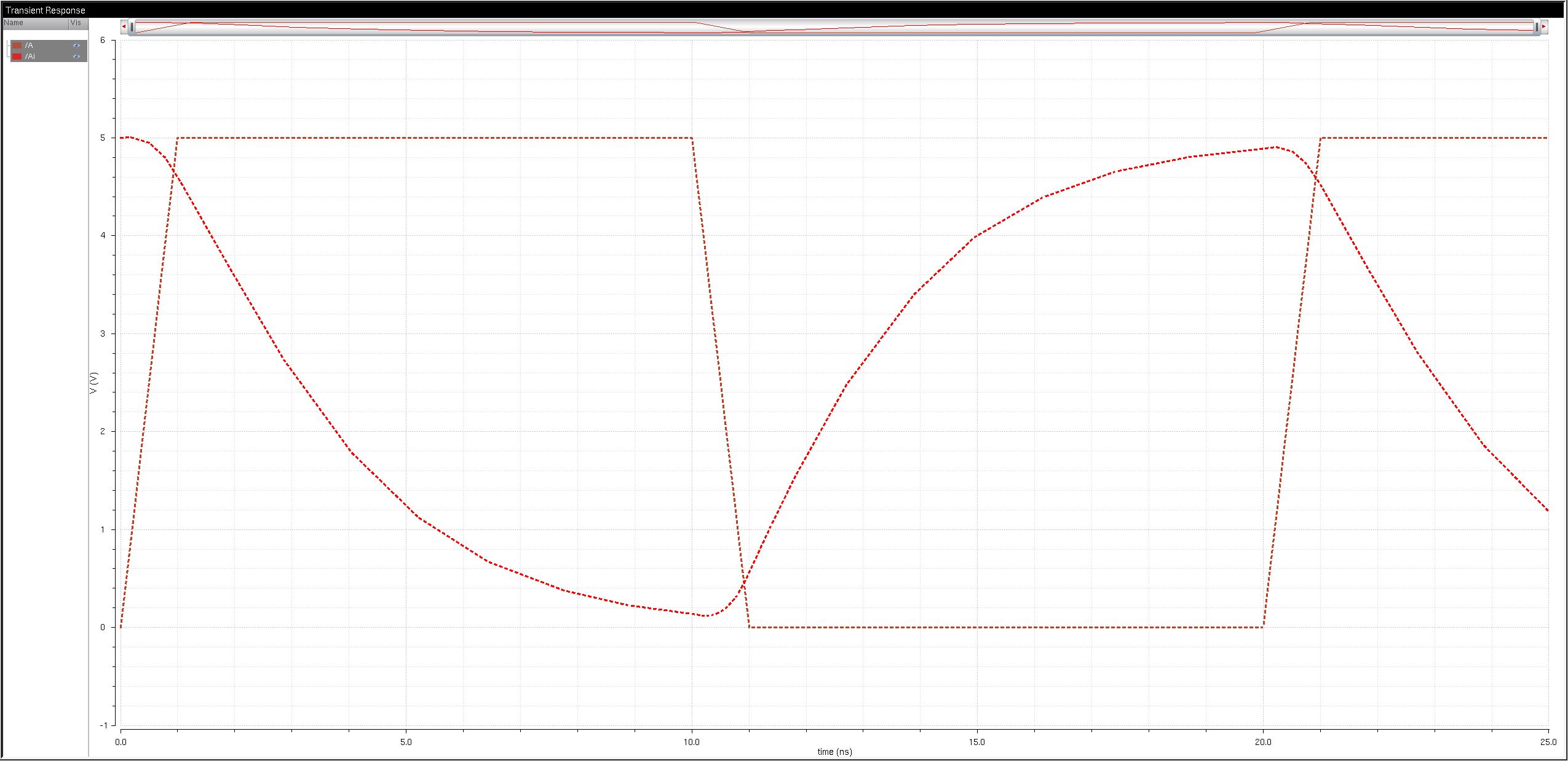
| 100pF Spectre | 100pF UltraSim |
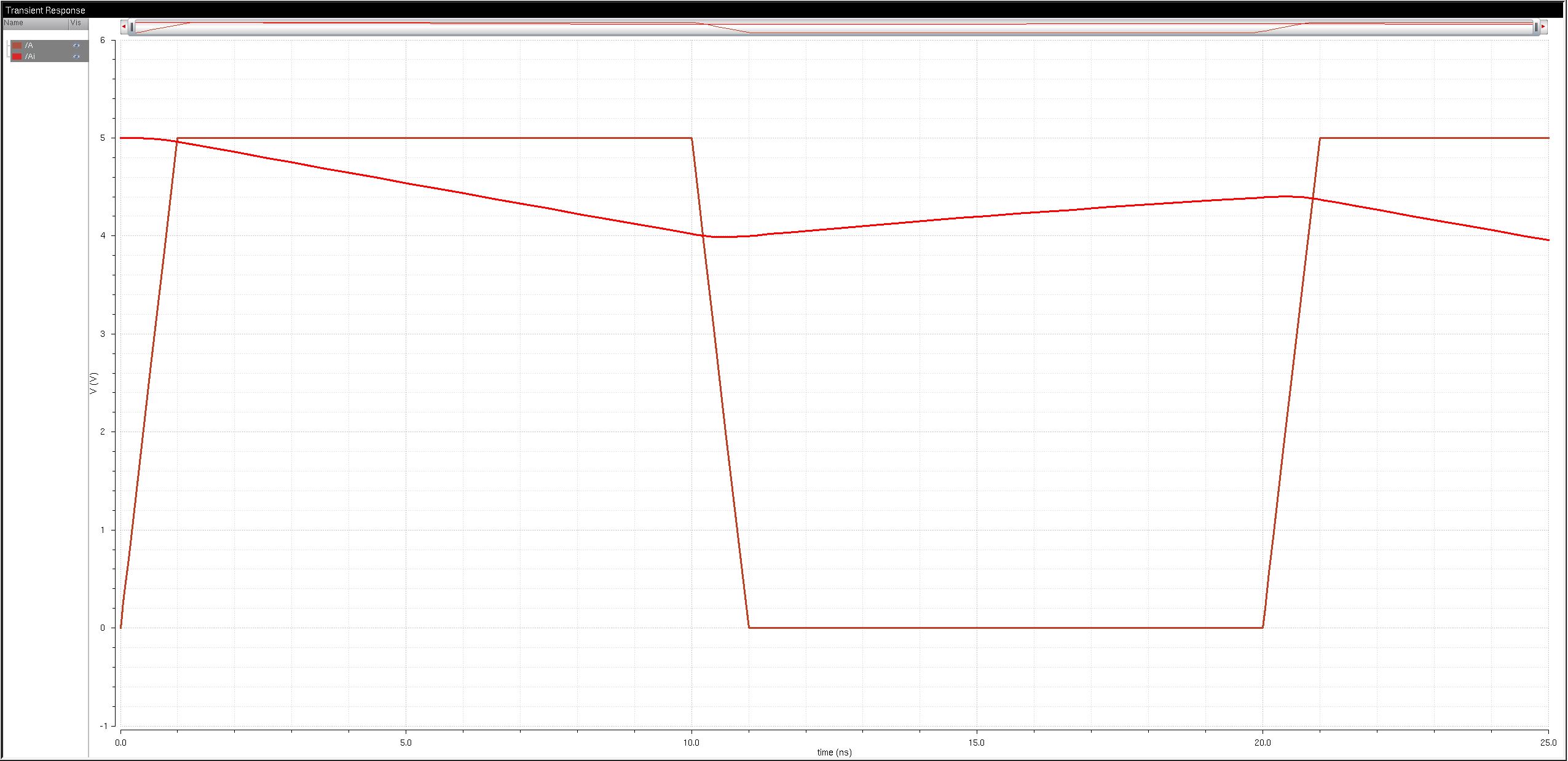
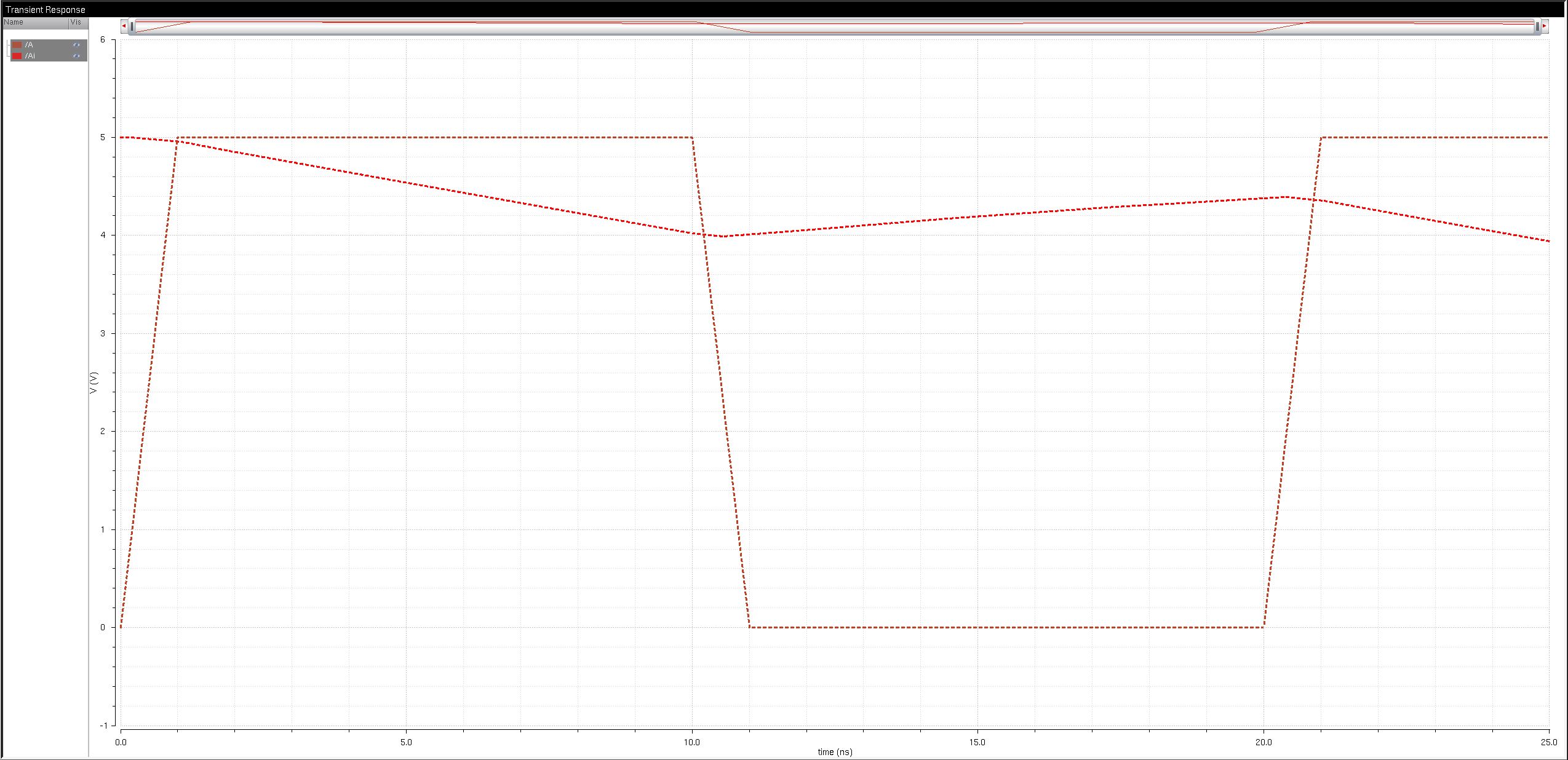
My design files used in this lab as well as the snips can be downloaded here.