Digital Integrated Circuit DesignEE 421L - Fall 2021
Lab 3
Author: Ryan Eclarinal
Email: eclarina@unlv.nevada.edu
Date Assigned: September 8, 2021
Due Date: September 15, 2021
Pre-Lab:
We were asked to finish the Tutorial 1 in making a 10K n-well resistor and use it to create a divider.
Schematic

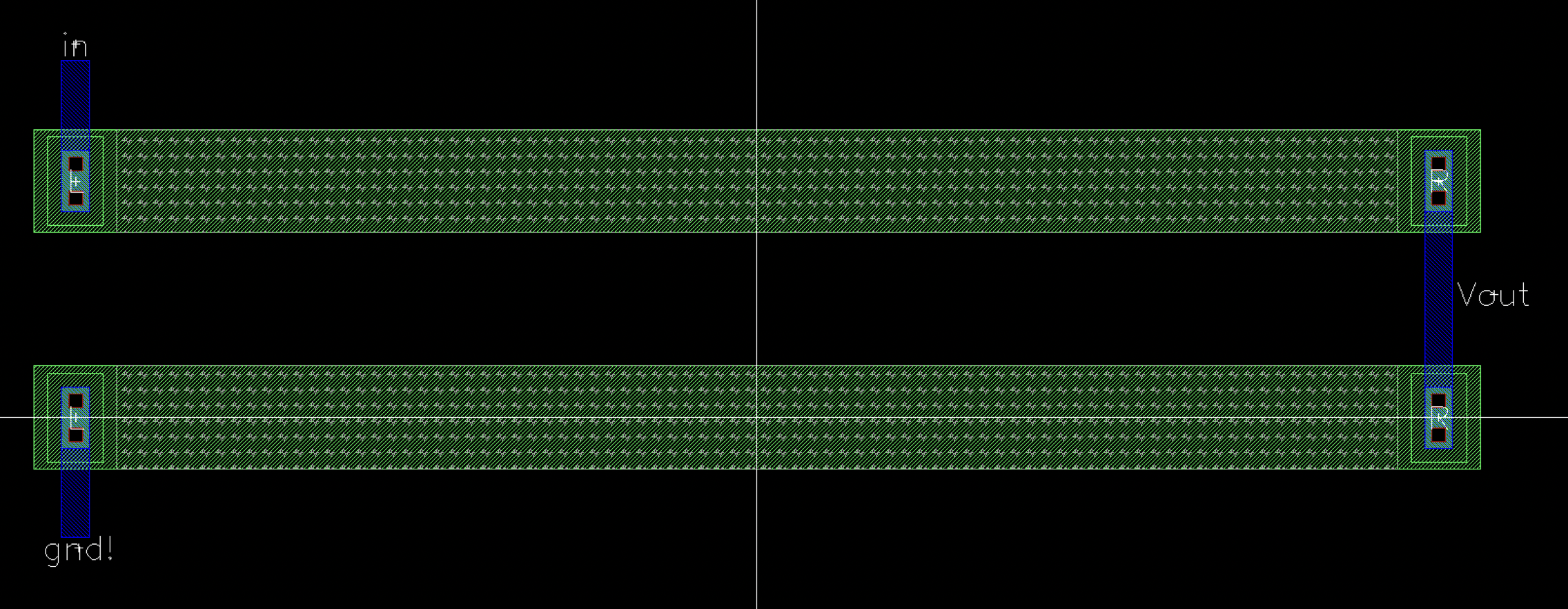
Layout of the 10K n-well resistor divider

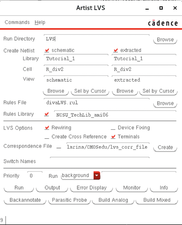
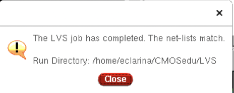
LVS and result


Lab 3 Description:
Layout of a 10-bit digital-to-analog converter (DAC)
Lab 3 Procedure:
This lab will focus on the layout of the 10-bit DAC you designed and simulated in Lab 2
- Use the n-well to layout a 10k resistor as discussed in Tutorial 1
- Discuss,
in your lab report, how to select the width and length of the resistor
by referencing the process information from MOSIS
- Use this n-well resistor in the layout of your DAC
- Discuss, in your lab report, how the width and length of the resistor are measured
- Ensure
that each resistor in the DAC is laid out in parallel having the same
x-position but varying y-positions (the resistors are stacked)
- All input and output Pins should be on metal 1
- DRC and LVS, with the extracted layout, your design
For this Lab, i created a new 10K n-well resistor referencing
the process information from MOSIS. For this resistor, i chose the 7.5
microns for the width and 91.65 microns for the length.

After extracting the layout, this was the value that i got for my resistor

Then, we will use the schematic of the 10-bit DAC that we created on Lab 2.
This is the beginning circuit

Schematic of the 10-bit DAC

Once
we have the schematics, we will then create a layout of our circuit
using the 10K n-well resistor and put it on a cell called 2R_R_.

After
creating the layout, we have make sure we DRC our layout to see if
we're getting some errors before we continue. If there is no error, we
may proceed.
We
will then create a new layout using 2R_R_ layout that we did. We will
use the 2R_R_ layout to create the 10-bit DAC that mirrors the
schematic of our design.

Pressing the bindkey E and changing the Display Level Stop to 0 will show what we have on our layout

DRC the layout and if there's no error, we can now extract our layout

We are now ready to LVS our design

After running the LVS, it will let us know if the net-lists matched.


And lastly, here are the results of LVS that we ran that shows we have successfully finished our layout/design.

The design file can be found here lab3.zip
Backing up:
Perform a regular back up of my work by making a zip file and uplaod it to my Google Drive.


Return to Students
Return to EE 421L
Return to CMOSedu.com
