Lab 3 - EE 421L
Damian Aceves-Franco
acevesfr@unlv.nevada.edu
09/14/2021
Layout of a 10-bit digital-to-analog converter (DAC)
Prelab
- Back-up all of your previous work from the lab and the course.
- Finish Tutorial 1 seen here.
The
rest of the tutorial 1 involves makeing an N-Well resistor (10K
each) in layout and and building the flowing circuit in
schematic layout and comeparing this schematic to the one in layout by
the use of LVS
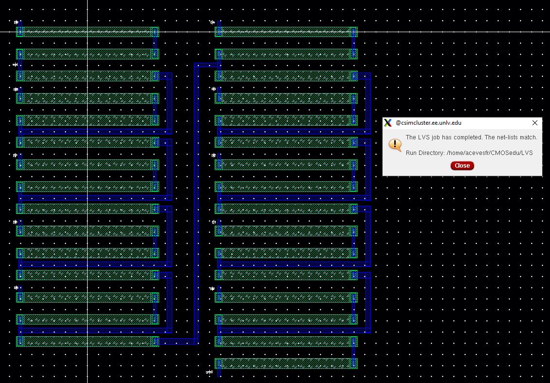
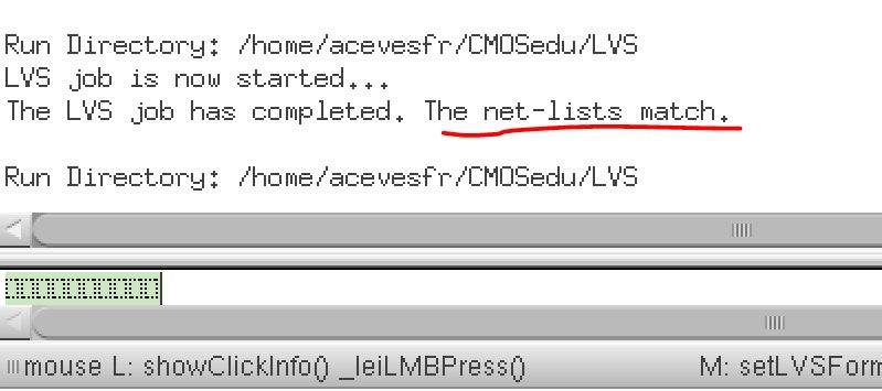
Now the layout and LVS ( if the net-list match) we were sucessful in making sure they are the same circuits.
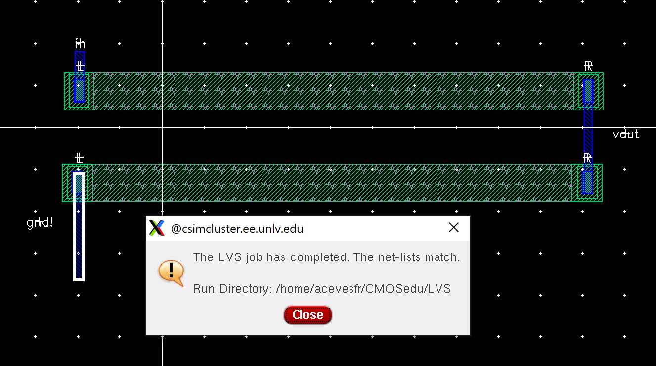
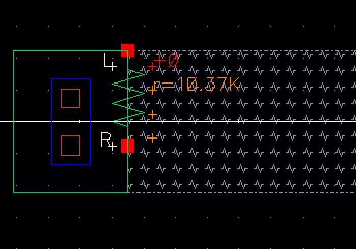
Extrating the layout shows us the value of the N-Well resistance I made.
*******************************************************************************************************************************************
Lab
This lab will focus on the layout of the 10-bit DAC you designed and simulated in Lab 2
- Use the n-well to layout a 10k resistor as discussed in Tutorial 1
- Discuss,
in your lab report, how to select the width and length of the resistor
by referencing the process information from MOSIS
- Use this n-well resistor in the layout of your DAC
- Discuss, in your lab report, how the width and length of the resistor are measured
- Ensure
that each resistor in the DAC is laid out in parallel having the same
x-position but varying y-positions (the resistors are stacked)
- All input and output Pins should be on metal 1
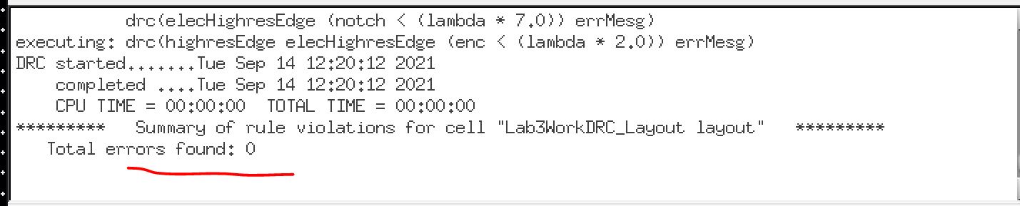
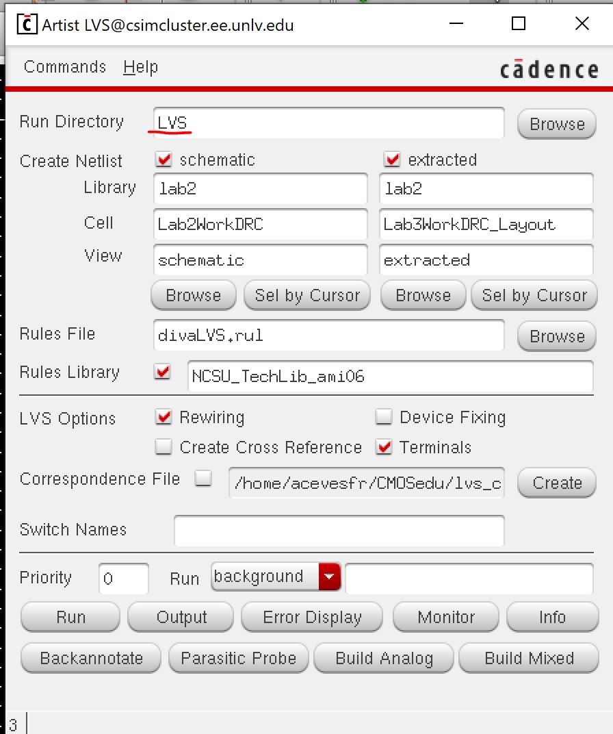
- DRC and LVS, with the extracted layout, your design (show the results in your lab report)
- Zip up your final design directory and place it in
the lab3 directory, with a link on your lab report, so the grader can
examine both the layout and schematic (and simulations)
**********************************************************************************************************************************************
Work
Use the n-well to layout a 10k resistor as discussed in Tutorial 1
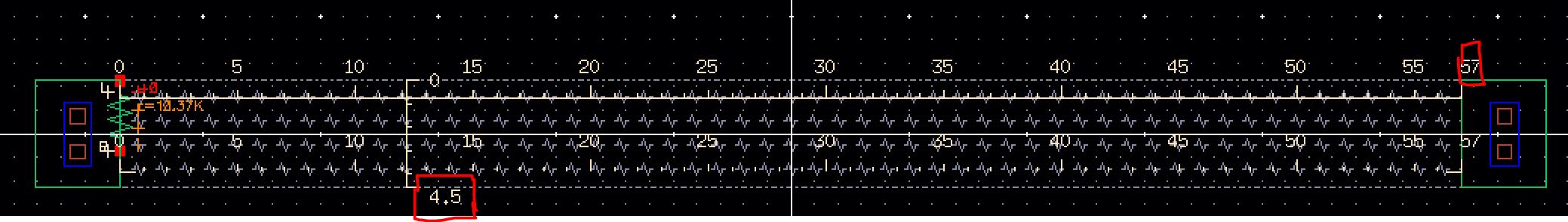
- lets say the width of the 10K resistor is 4.5um and we want to find out with the lenght would be with we do this by
using the formula
R= Rper-square* L
W
we
know by the table provied here the Rpersquare is about 855 or
about 800 ohms/square. So 10K= 800 * L/4.5 => L= 56.25+0.3 ~57
Use this n-well resistor in the layout of your DAC
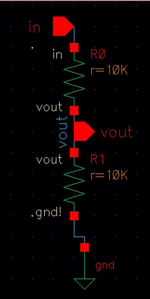
This the schematic view of the circuit.
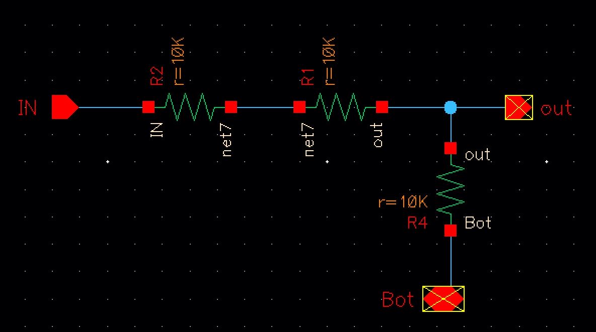
after making it into a symbole we get this
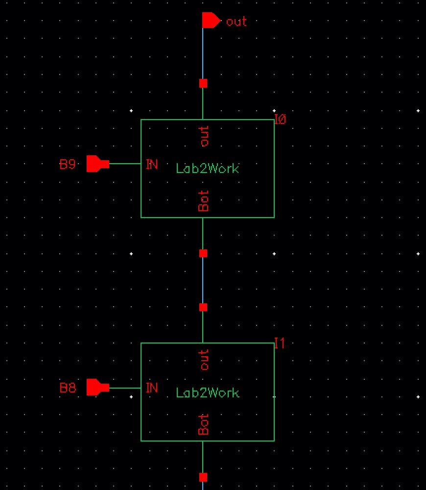
As we did in Lab 2
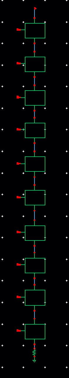
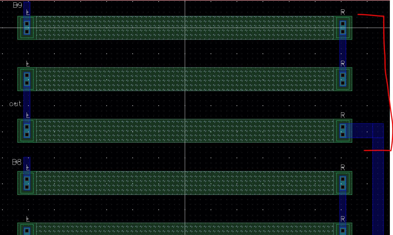
We
place the 10K N-well I this configuration to get the same type of
circuit as in schematic view and making them have the proper spacing of
5.40um between them. As well we must name the pin the same and
place them were they need to be and wire everything up with metal1.
-
after doing we DRC and LVS it as we did in the prelab to make sure everything lines up and its working properly
Backing up the work
Below are the files for this lab
ZipFile.
Return to Labs