Lab Final Project - High Speed Digital Receiver
Author: William Wherry
Email: wherrw1@unlv.nevada.edu
11/18/2020
Lab
description:
- Design,
layout, and simulate a digital receiver circuit that accepts
a high-speed digital input signal D and Di (a differential pair
connected to your circuit from, for example, a twisted pair wires such as in an Ethernet cable).
- D
and Di are complements so, for example, if D is 5V then Di is 0V and
output = 1. Another example, when D is 1V and Di is 2Vthen
output = 0. At high-speeds and long distances the voltages received
aren't full digital logic levels (i.e., 5V and 0V), hence the need to
design, and use, a high-speed digital recevier circuit.
Ideally, when D > Di the receiver outputs a 1. When D < Di
the receiver outputs a 0. Base your design on
the topology seen in Fig. 18.23.
- Try to design for high-speed and low-power. Characterize your design (in sims) and the trade-offs.
For example, show that you get higher-speed if you use more energy
(burn more power). See if you can get, in this 500 nm process, 250
Mbits/s (a bit width of 4 ns) with an input voltage difference of, for
example, 250 mV (with D and Di swinging back and forth between 2.75V
and 3V, for one of many examples, your circuit outputs the
correspondingly correct values). Note that while Fig. 18.23 shows one
inverter on the output you may find, for example, that two
inverters work better (at the cost of power). Use a table to summarize
your design's performance.
Final Project Design:
Utilizing the design shown in CMOS Circuit Design, Layout, and Simulation, Fourth Edition , fig
18.23 utilizes an NMOS flavor differential amplifier in parallel with a
PMOS flavor differential amplifier to create a high speed input buffer.
Attached to the output is an inverter that helps "square up" the rising
and falling edges of the output waveform. The circuit is designed to
take the difference of two input signals, a signal and its inverted
signal in this case, and amplify the difference between them. This
functionality perfectly fits the requirements of this project, so I
decided to build my design based on this circuit. The book's example of
the circuit uses 10/1 NMOS and 20/1 PMOS as default devices, since the
electron mobility is a little different for the PMOS's, so we need to
give them extra width in order for their internal MOSFET resistance Rp
to be as close to the NMOS's resistance, Rn, as possible. This also
helps to give a switching point voltage as close to the VDD/2 as
possible, so that we can slice our signals correctly and get good
output digital logic signals.

Baker, R. J. (2019). CMOS: Circuit design, layout, and simulation. Hoboken, NY: John Wiley & Sons.
Since
the goal of this project is to have as fast a circuit as possible, with
as low of power as possible, it was important for me to keep the
propogation delays tPHL and tPLH as low as possible. With this in mind,
I had to find a balance between a sharp digital logic output signal and
the delays that would be caused by chaining together more inverters in
pursuit of that sharp signal. I noted that adding two inverters to the
book's design would sharpen the signal and keep it outputting a
non-inverted signal, but I decided to instead swap the D and Di inputs
in order to use one less inverter to save some speed that would be lost
with the third inverter. My first basic schematic design is shown
below.

Please
note that this was not my final design, just the starting point. I made
a symbol for the design to make it easier to simulate as seen below.

Next,
I wanted to do some simulations to see if it actually functioned as it
was supposed to. I used two simple voltage pulse sources to simulate an
attenuated signal over a long distance. Specifically, I set the
voltages between 2.75V and 3V, which are the minimum voltages required.
I figured if it worked in this worse case, then I could move on from
there to make it more efficient. I
also tested the best case scenario of 5V to 0V (no attenuation) as well
as a voltage swing between 2.9V and 3V to see if it would work at that
low of a voltage.

THESE ARE JUST TO TEST THE BASE CIRCUIT FROM THE BOOK. Comprehensive testing will be later in the report on my finalized circuit.
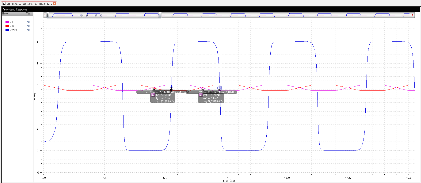
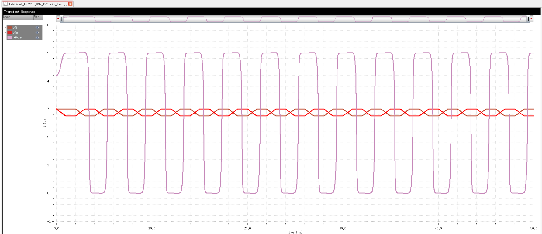
First test: 3ns bit width (333.3Mbit/s), 5V to 0V:

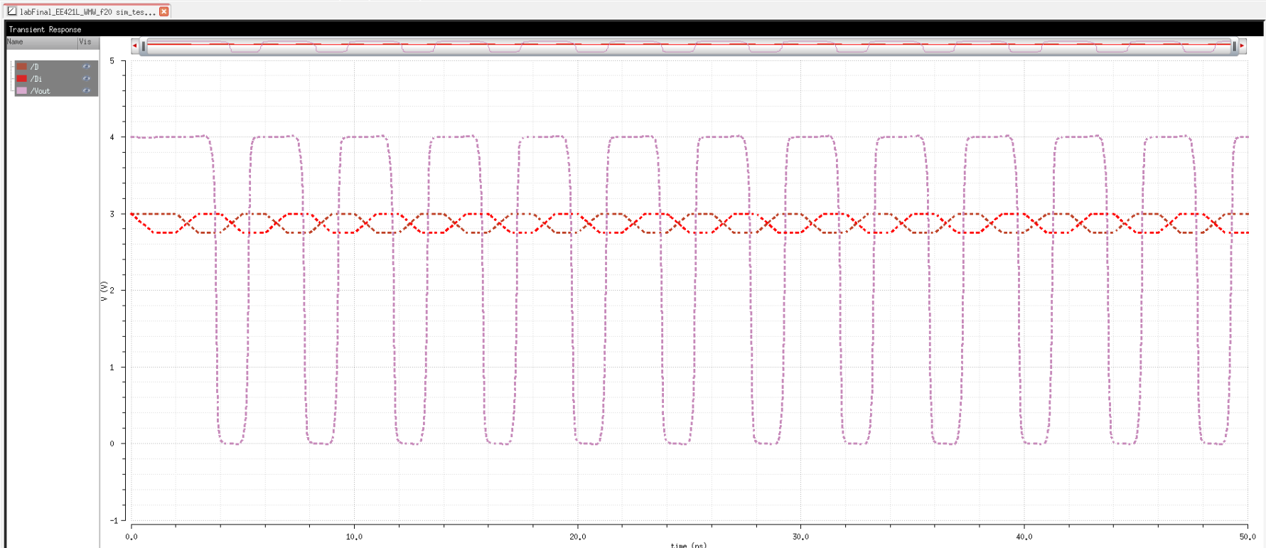
Second test: 3ns bit width (333.3Mbit/s), 2.75V to 3V:


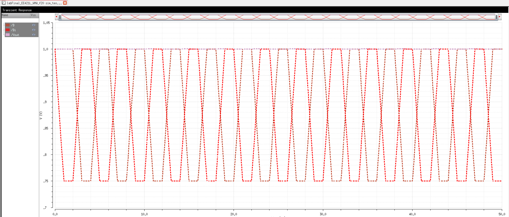
Fourth test, 3ns bit width (333.3Mbit/s), 2.9V to 3V (100mV amplitude):

Fourth test: 1ns bit width (1Gbit/s), 2.75V to 3V (250mV amplitude):


Data of note:
| Input signal | Bit Width | tPLH | tPHL |
| 5V to 0V | 3ns | 375.6ps | 386.2ps |
| 2.75V to 3V | 3ns | 716.7ps | 731.0ps |
| 2.75V to 3V | 1ns | 731.8ps | 724.4ps |
You
can see here that the base circuit has good tPHL and tPLH
propagation delays
right out of the box, even at 1ns bit width or 1Gbit/s, and the output
digital signal is fairly sharp and reaches full digital logic levels.
The circuit even seems to work as low as 100mV (thanks to the parallel
PMOS and NMOS flavor dif amps the inputs can be theoretically rail to
rail), although that is less than the required minimum, so I will not
test that further.
With such decent delays, there is a lot of room for improving power
dissipation at the cost of speed. The easiest way in the case of this
circuit to improve power dissipation is to increase the length of the
top-most PMOS and bottom-most NMOS in the circuit. This will lower the
speed, current use, and power use.

Judging
by the trials above, it appears that I will get the most propagation
delay at very low input voltages. Therefore, I decided the easiest way
to test different lengths of MOSFET to try to save power at the cost of
speed was to use the worst case scenario of a greatly attenuated 250mV
input, since it had the greatest delays. Since I know that the base
circuit can get down to 1ns bit width without much issue, I decided to
use that as my goal. Also, since I was using 1ns rise and fall times in
my simulation, I wanted the delays to be less than that if possible. I tested a few different sizes using
a very low bit width and you can see the results below.
In an effort to not clutter the page, I only show the pictures of the
base circuit simulations compared to my pick of the best compromise
between power dissipation and propagation delay and put results of
others in the table only.
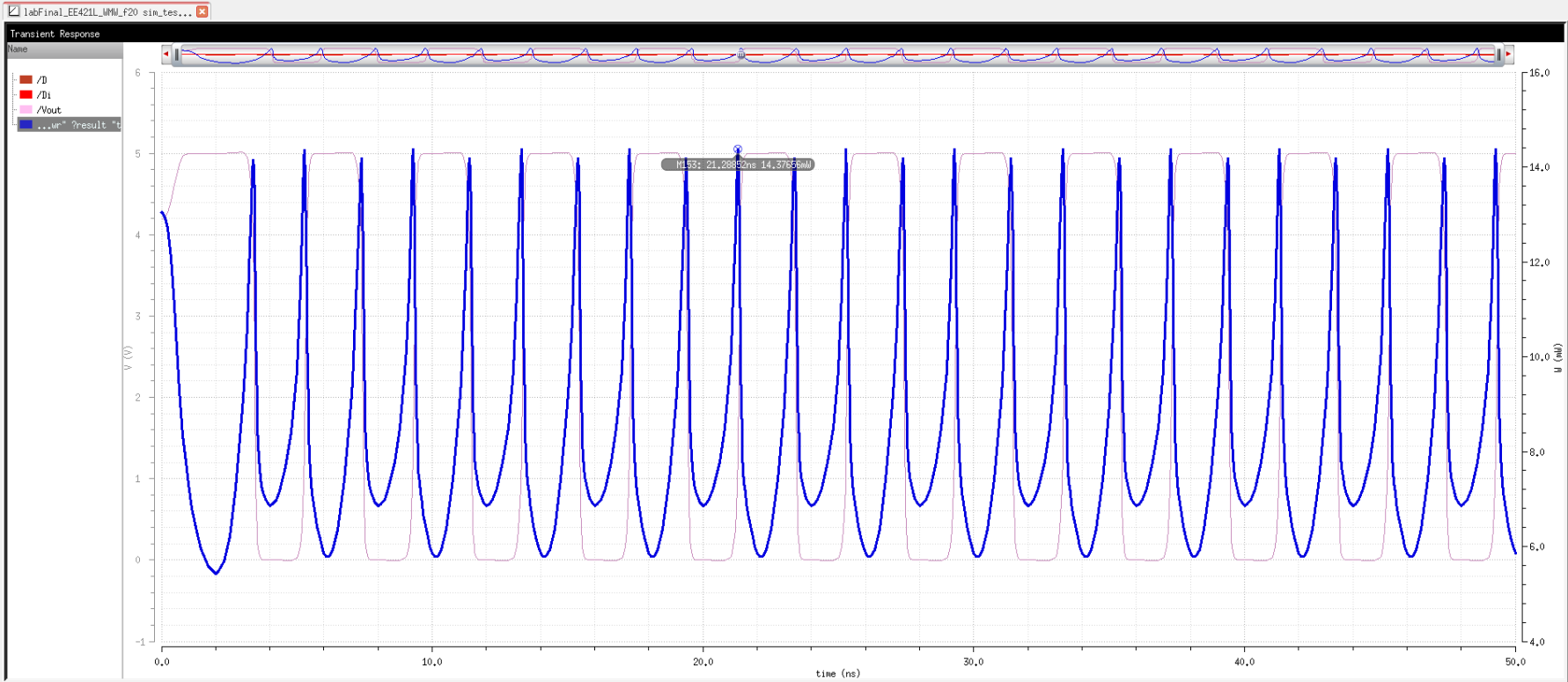
Base circuit simulations (click image to enlarge):


Final choice simulations (click image to enlarge):


| Input | Bit width | NMOS W/L & PMOS W/L | tPLH | tPHL | Average Power over 50ns |
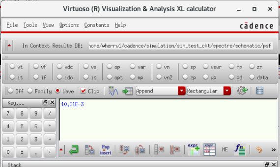
| 3V to 2.75V (250mV) | 1ns | 6u/0.6u & 12u/0.6u (Base circuit) | 731.8ps | 724.4ps | 10.21mW |
| 3V to 2.75V (250mV) | 1ns | 6u/6u & 12u/6u | 998ps | 1250ps | 5.3mW |
| 3V to 2.75V (250mV) | 1ns | 6u/6u & 12u/0.6u | 781ps | 890ps | 7.2mW |
| 3V to 2.75V (250mV) | 1ns | 6u/3u & 12u/3u | 952ps | 1027ps | 5.27mW |
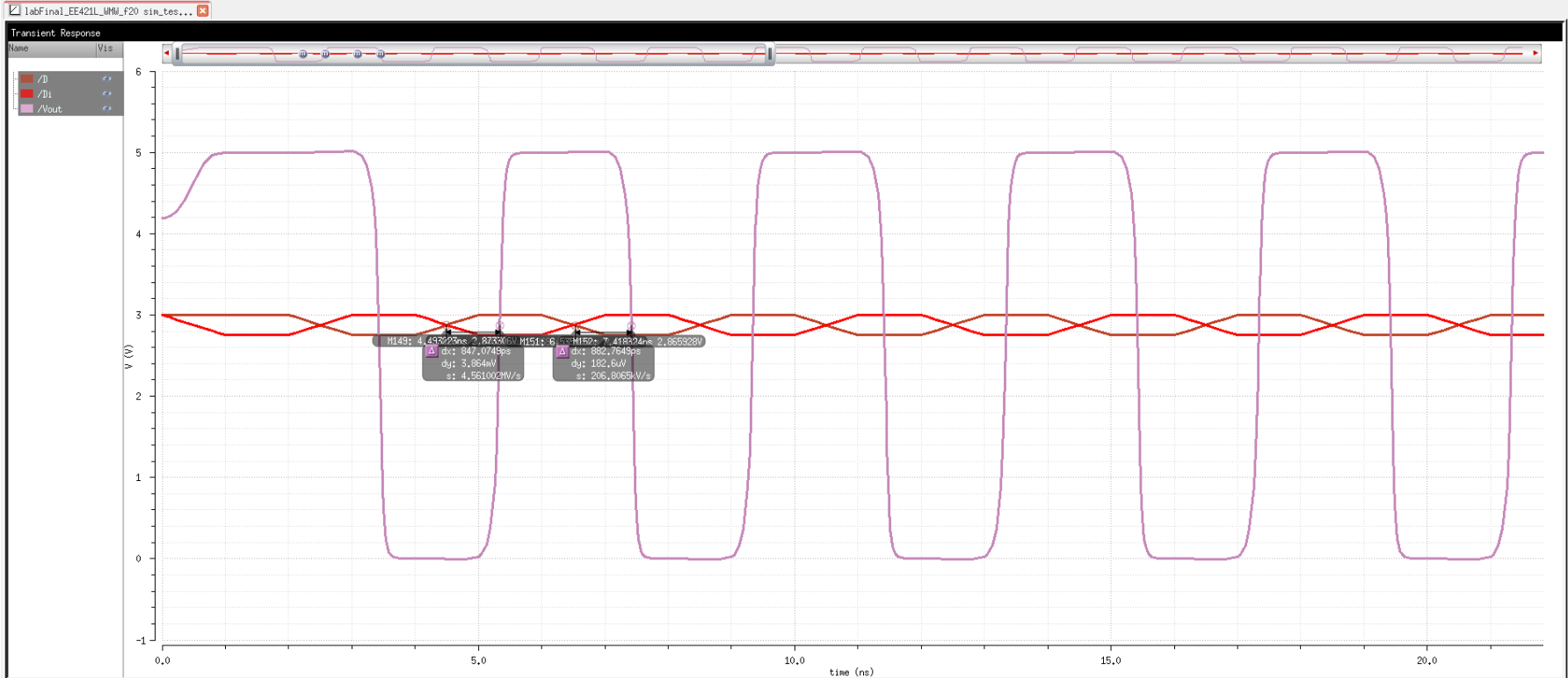
| 3V to 2.75V (250mV) | 1ns | *12u/2.1u & 12u/3u | 847ps | 882ps | 8.2mW |
*Through
testing, I found that the tPHL can be adjusted with the PMOS W/L and
the tPLH can be adjusted with the NMOS W/L, so I managed to get the
delays to similar values while reducing power consumption.
Judging
by the delays and the average power over 50ns, I decided that my final
design would use an uppermost PMOS of 12u/3u and a lowermost NMOS of
12u/2.1u. This combination gave good propagation delays that are close
to each other in value, while staying under the 1ns goal that I set for
myself and also saves about 20% power over the base circuit on average.
The final circuit schematic is shown below.
Final Design:

With
my candidate for a final design decided, I needed to do more testing to
look at the characteristics of the design. First, I wanted to
performance of several bit widths and voltage levels to be positive it
behaves as it should. Below are several trials with their results
summarized in a table.
TESTING DIFFERENT BIT WIDTHS AND INPUT VOLTAGES:
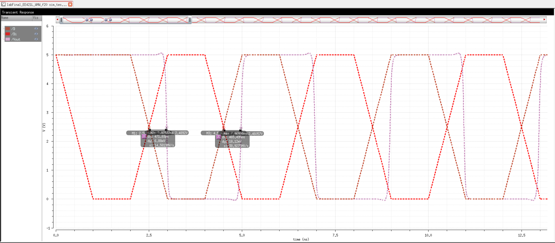
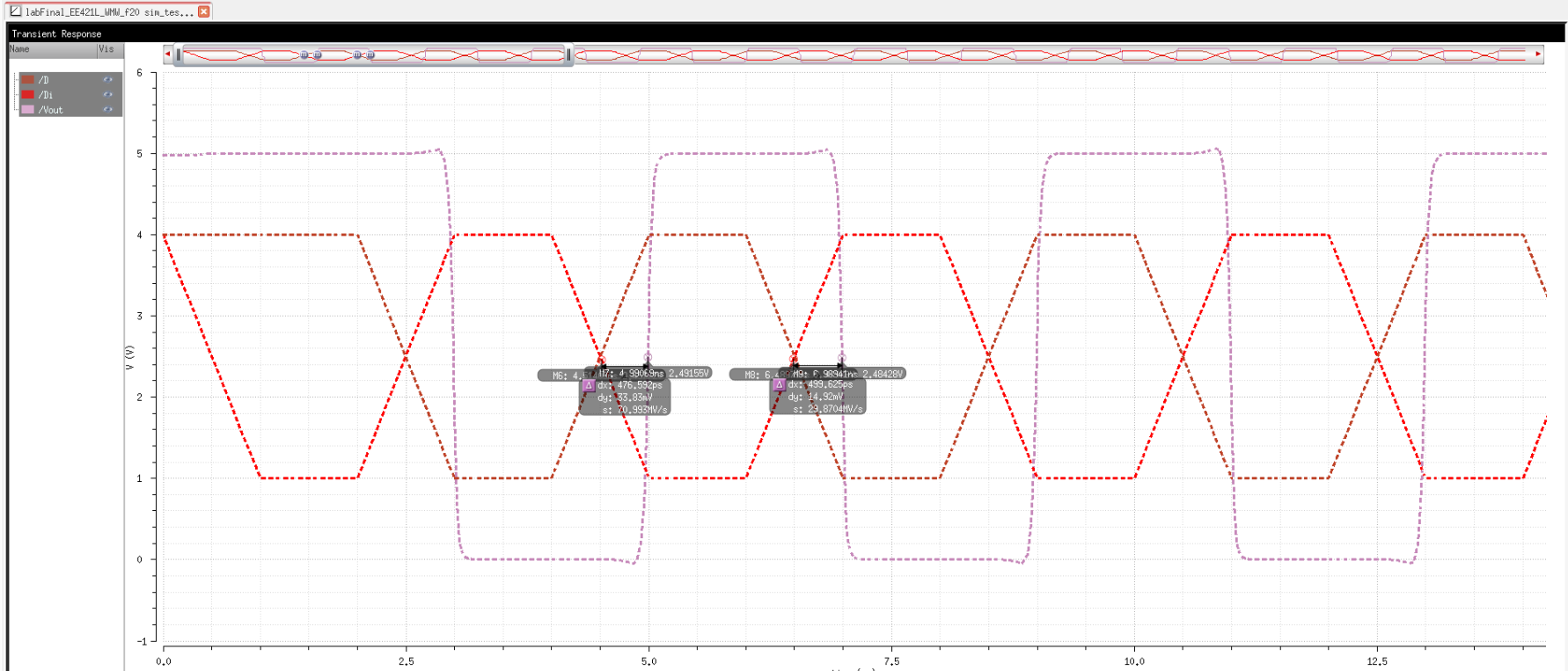
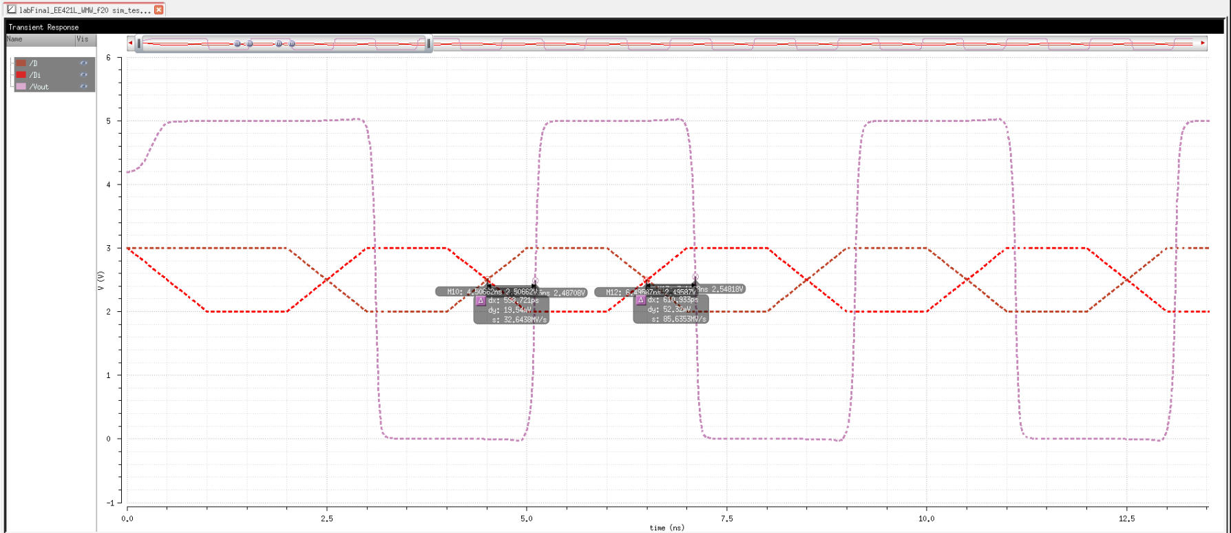
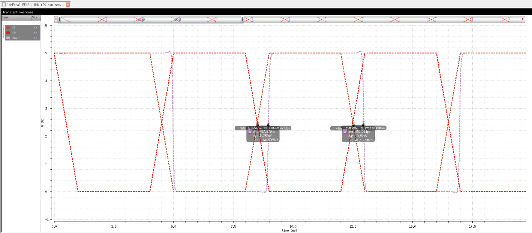
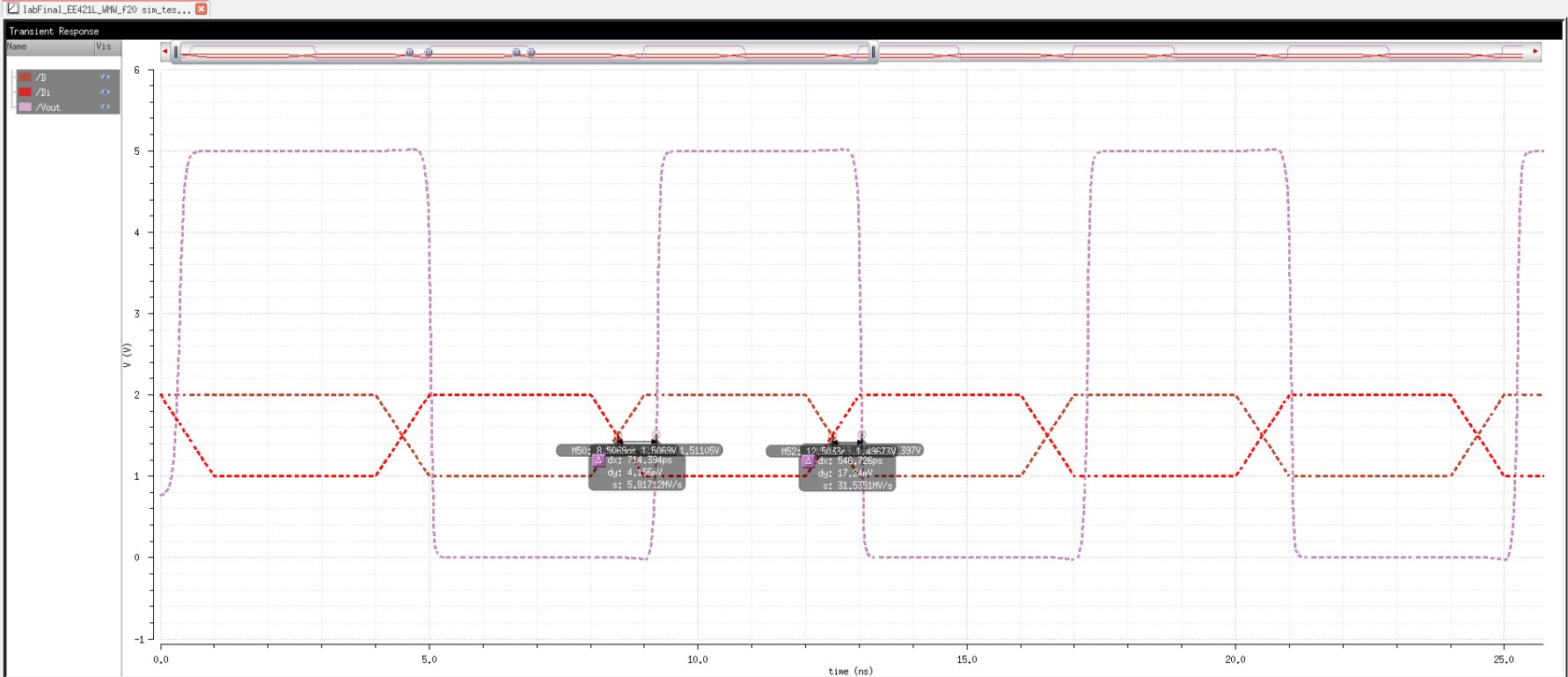
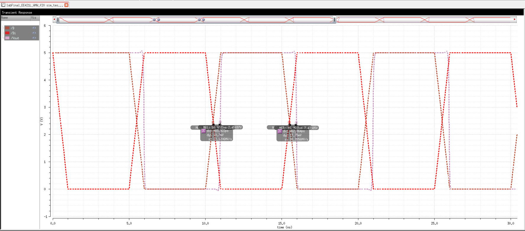
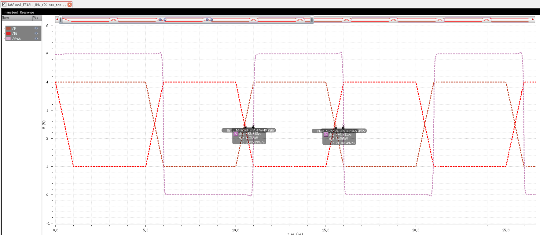
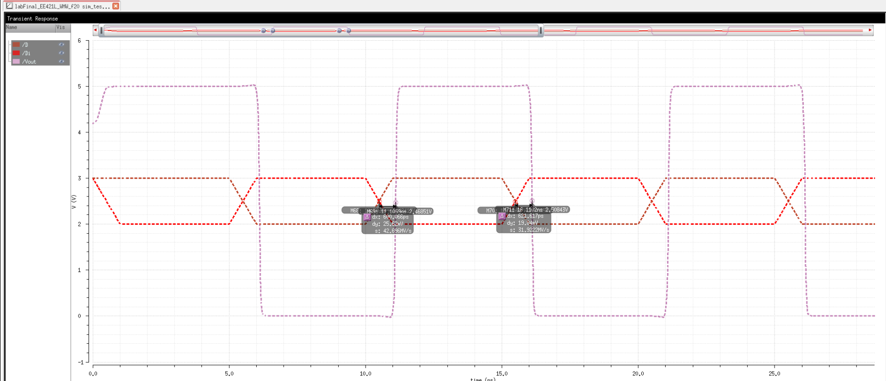
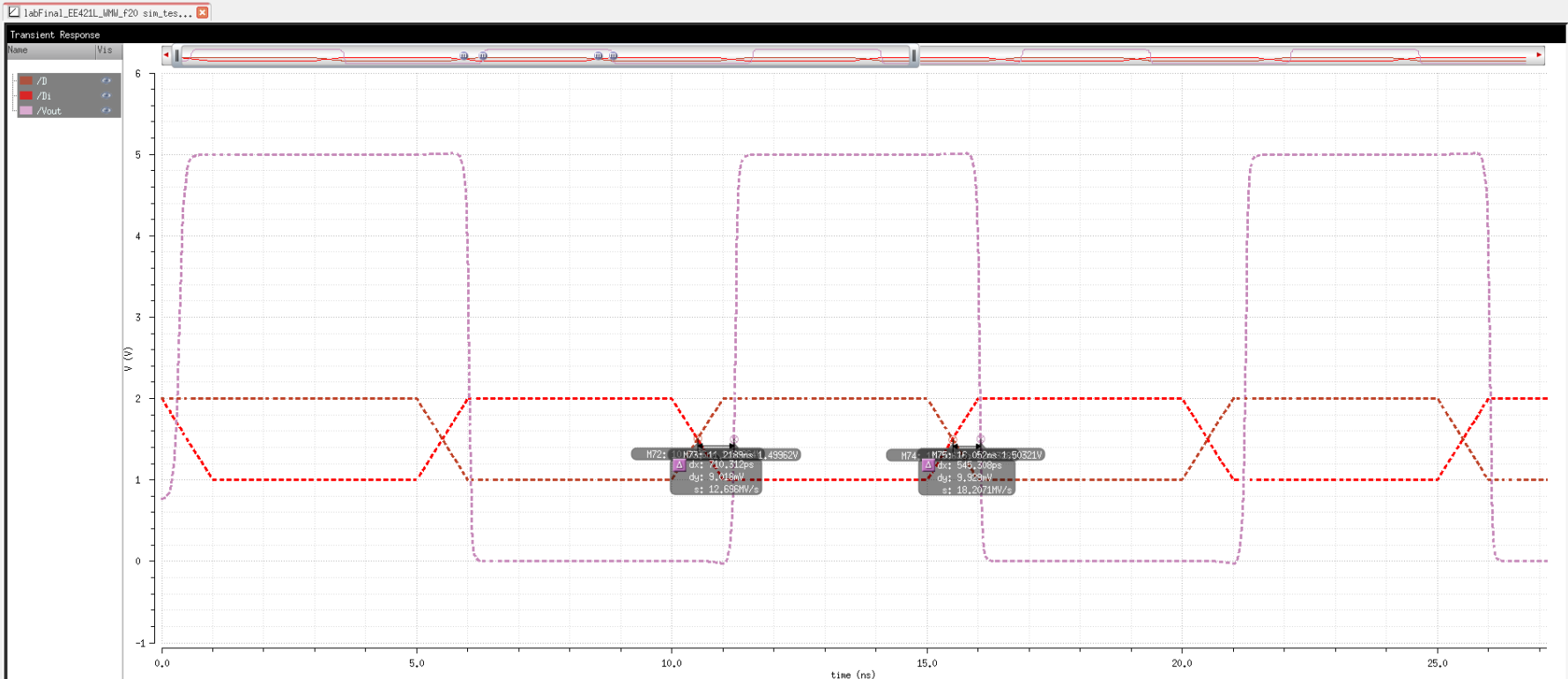
1ns bit-width (1Gbit/s):
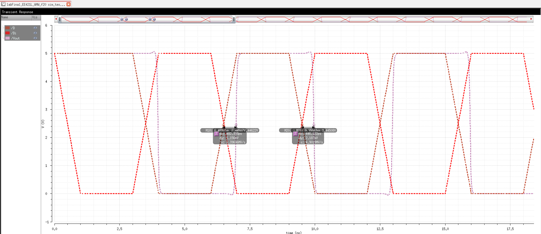
5V to 0V:


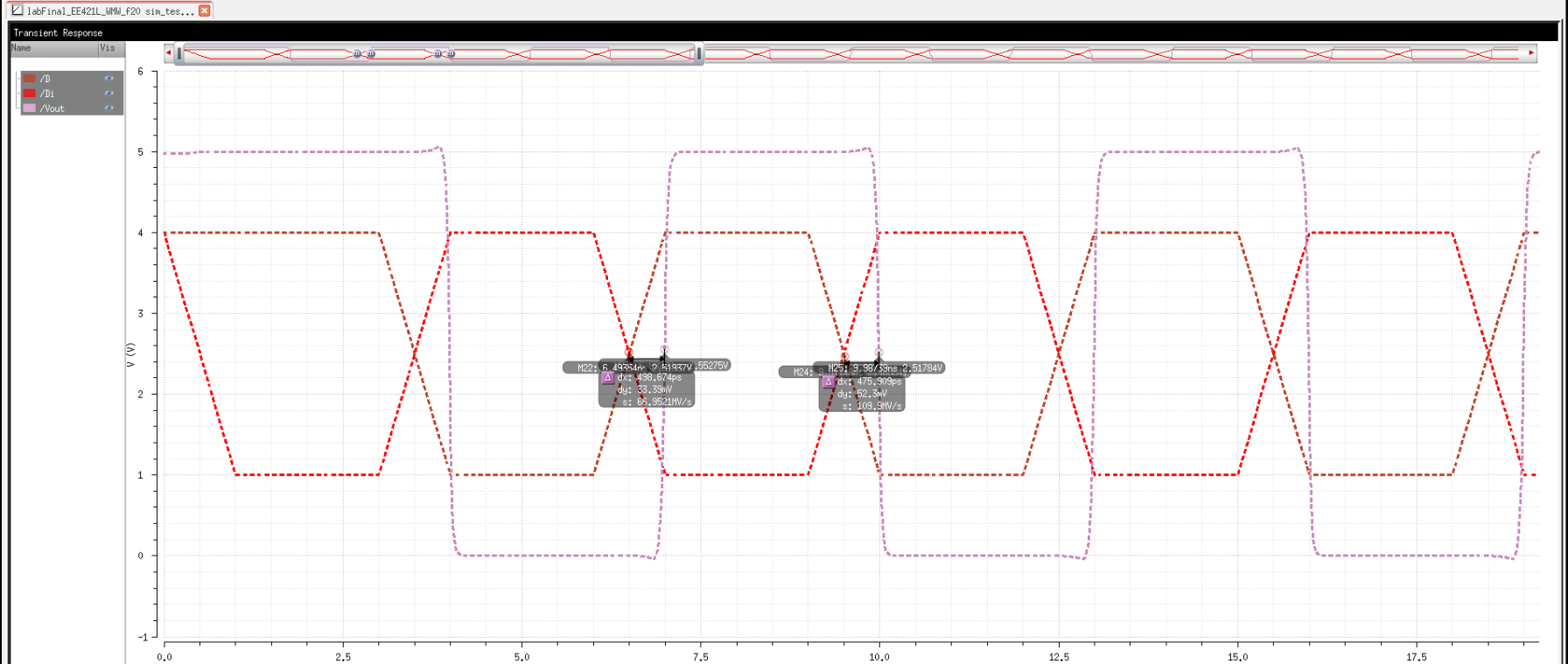
4V to 1V:


3V to 2V:


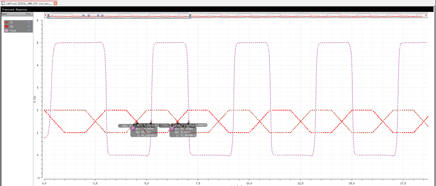
2V to 1V:


3V to 2.75V:
| Input Signal | tPLH | tPHL | Avg Power over 50ns |
| 5V to 0V | 471.8 ps | 465.5 ps | 4.99mW |
| 4V to 1V | 476.6 ps | 499.6 ps | 5.20mW |
| 3V to 2V | 598.7 ps | 610.9 ps | 6.22mW |
| 2V to 1V | 714.8 ps | 562.5 ps | 5.16mW |
| 3V to 2.75V | 847.0 ps | 882.0 ps | 8.20mW |
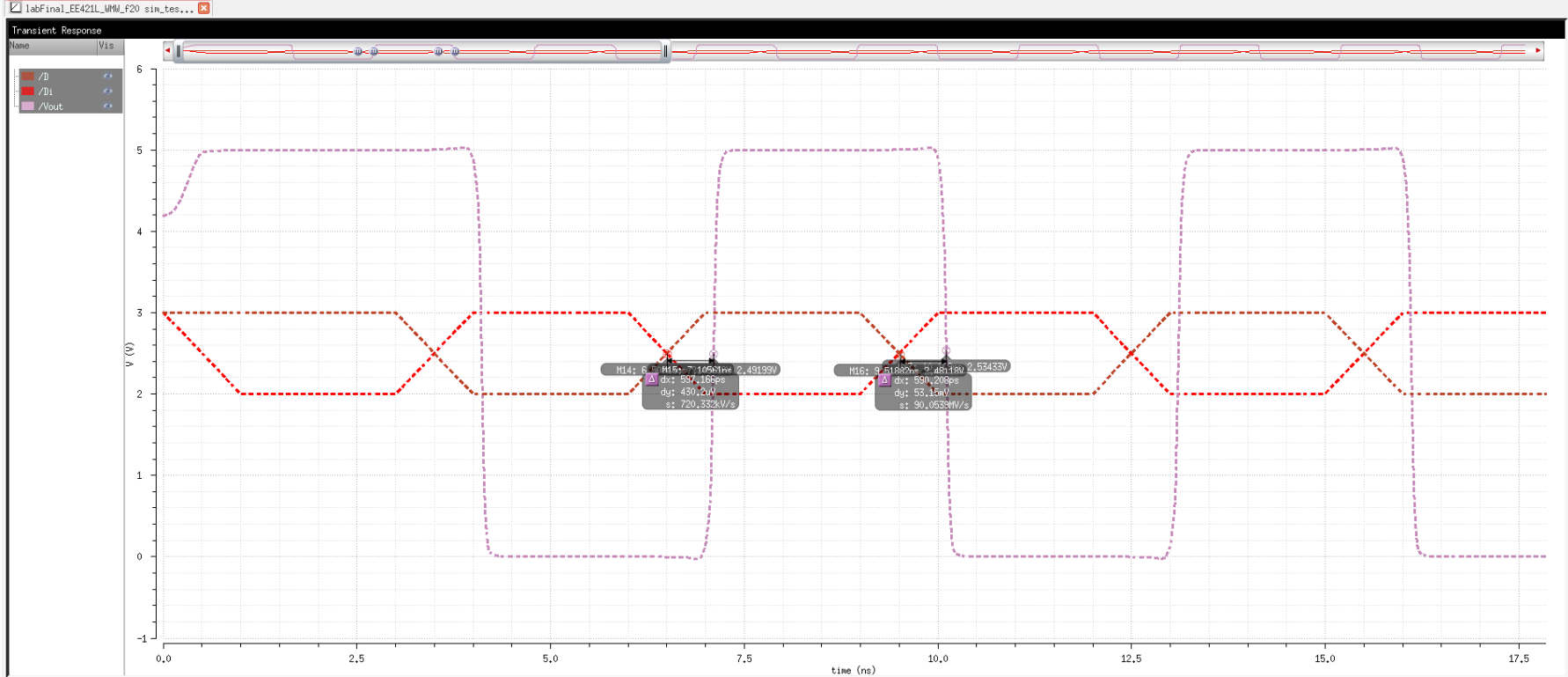
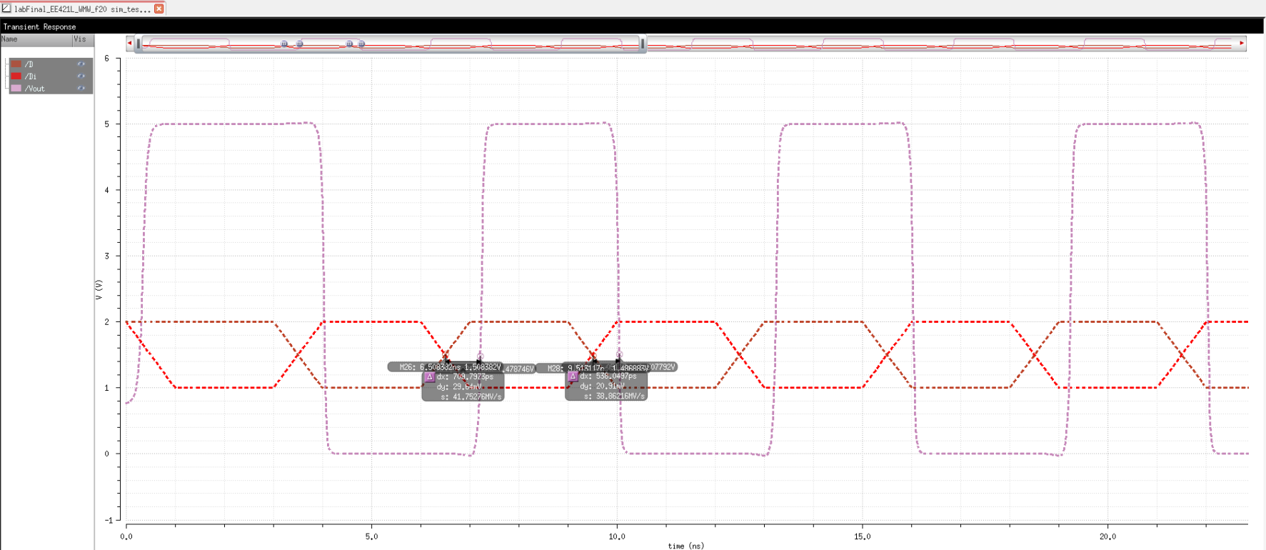
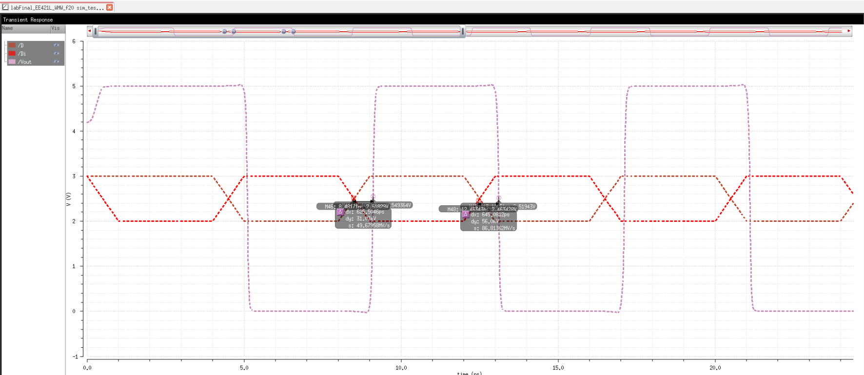
2ns bit-width (500Mbit/s):
5V to 0V:


4V to 1V:


3V to 2V:


2V to 1V:


3V to 2.75V:


| Input Signal | tPLH | tPHL | Avg Power over 50ns |
| 5V to 0V | 482.4 ps | 446.1 ps | 4.28mW |
| 4V to 1V | 498.7 ps | 475.9 ps | 4.56mW |
| 3V to 2V | 597.2 ps | 590.2 ps | 5.78mW |
| 2V to 1V | 709.8 ps | 538.0 ps | 4.75mW |
| 3V to 2.75V | 875.6 ps | 912.2 ps | 7.52mW |
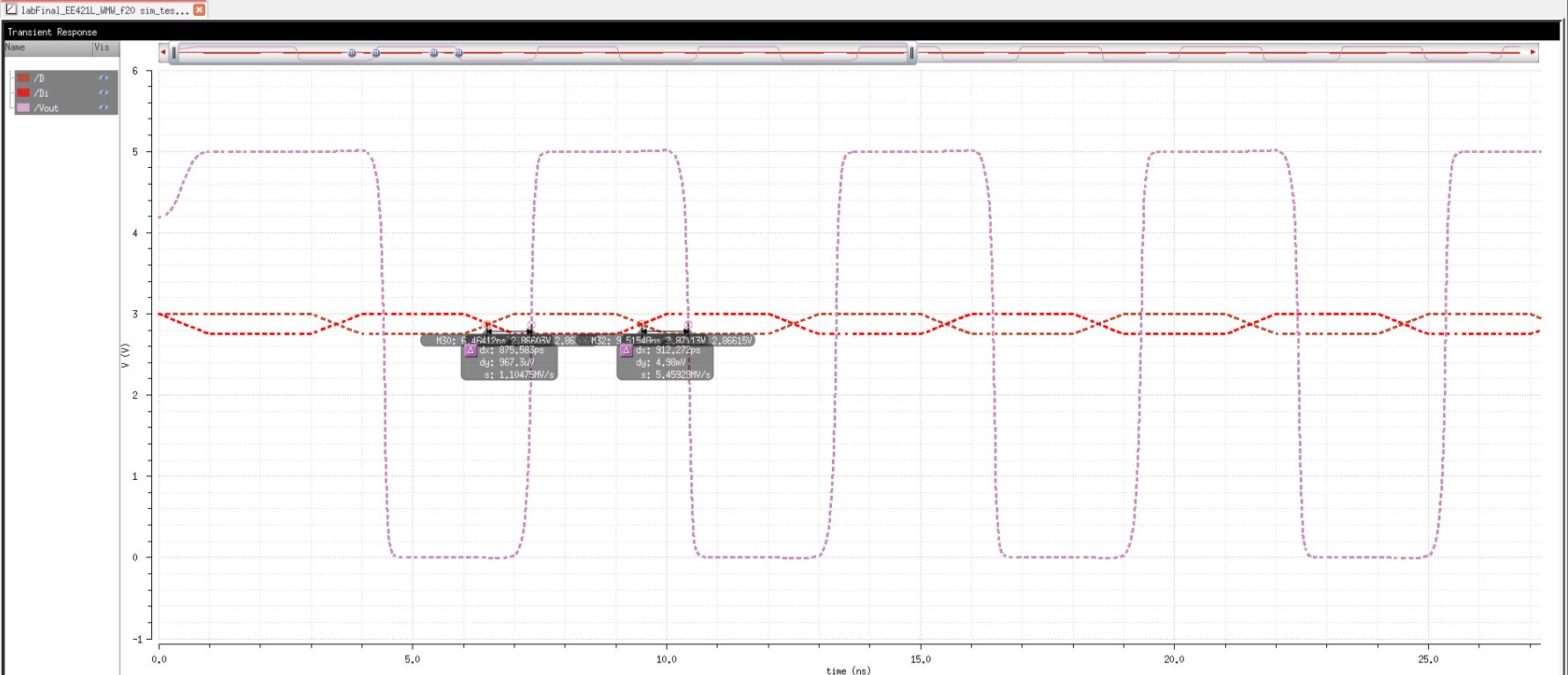
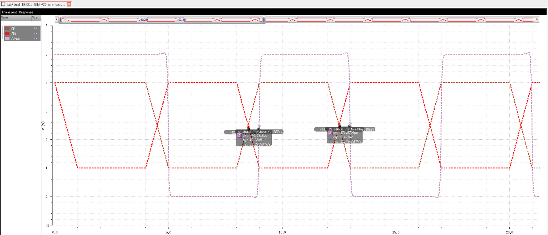
3ns bit-width (333.3Mbit/s):
5V to 0V:


4V to 1V:


3V to 2V:


2V to 1V:


3V to 2.75V:


| Input Signal | tPLH | tPHL | Avg Power over 50ns |
| 5V to 0V | 467.9 ps | 450.2 ps | 3.91mW |
| 4V to 1V | 585.3 ps | 471.6 ps | 4.24mW |
| 3V to 2V | 625.5 ps | 645.1 ps | 5.57mW |
2V to 1V
| 714.4 ps | 546.7 ps | 4.55mW |
| 3V to 2.75V | 820.0 ps | 923.0 ps | 7.19mW |
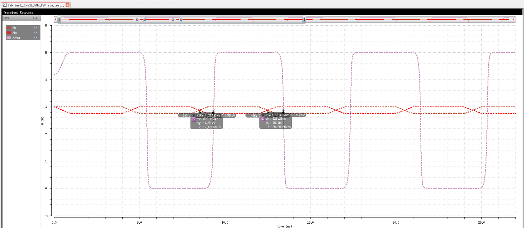
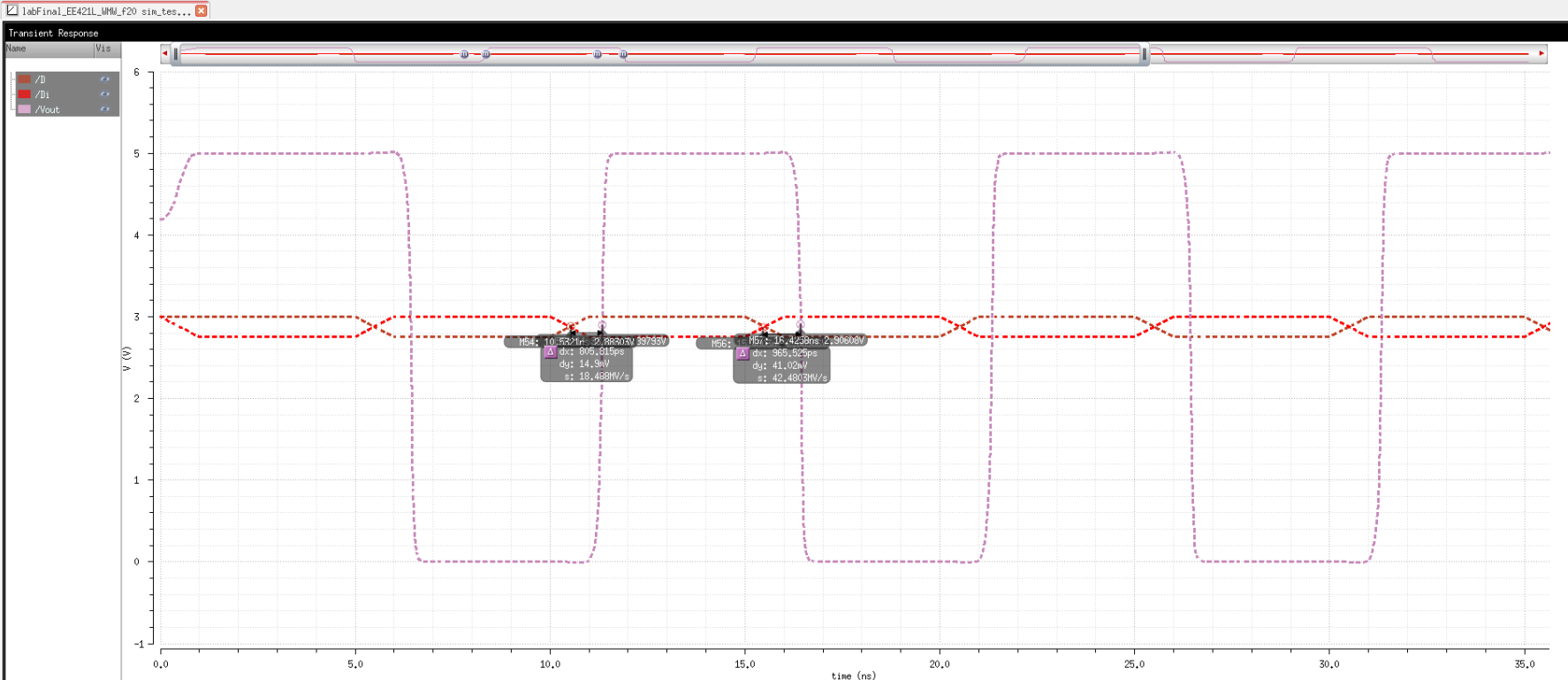
4ns bit-width (250Mbit/s):
5V to 0V:


4V to 1V:


3V to 2V:


2V to 1V:


3V to 2.75V:


| Input Signal | tPLH | tPHL | Avg Power over 50ns |
| 5V to 0V | 483.9 ps | 462.4 ps | 3.61mW |
| 4V to 1V | 483.3 ps | 470.7 ps | 3.98mW |
| 3V to 2V | 600.1 ps | 621.6 ps | 5.41mW |
2V to 1V
| 710.3 ps | 545.3 ps | 4.39mW |
| 3V to 2.75V | 805.8 ps | 965.5 ps | 6.94mW |
If you look closely at the average power dissipation across all bit widths, you can see that
in general the circuit consumes much more power as the input signal
gets smaller in amplitude. It appears to be much more efficient when
the input signal is larger, consuming almost half the power of that the
worst-case input does. Also, as the input signal gets smaller, the
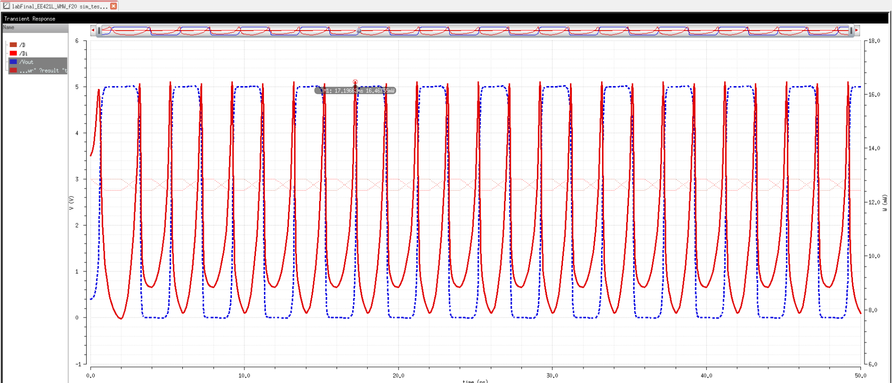
propagation delays increase dramatically. Finally, power dissipation also increases as speed increases. You can see this fact in the equation Pavg = Iavg * VDD = Ctotal * VDD^2 * freq_clk. Frequency
in this equation is related to the speed of the circuit, which
increases the power consumption of the circuit as speed increases. To
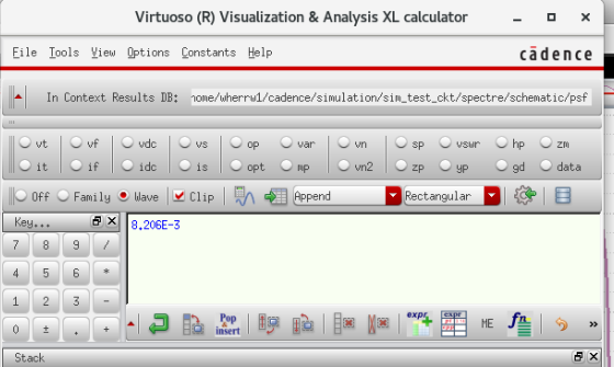
record the average power of the circuit, I used Cadence's built in
tools to find the instantaneous power over my 50ns transient
simulations and then used the average function in the calculator to find the average power consumption over that time period.
Next,
I tested temperature performance using a parametric analysis. I used the worst case 3V to 2.75V
input as well as the best case 5V to 0V just in case behavior changed
too much in one of these extreme cases. I assumed if these two
situations worked, then likely all in between would also be fine.
Temperature simulation from 0ºC to 100ºC with input voltage between 3V and 2.75V:

Temperature simulation from 0ºC to 100ºC with input voltage between 5V and 0V:

You
can see from the two graphs that in both cases, output propagation
delay increases as temperature increases. Both 250mV swing input and 5V
swing input still functioned, but both had increases in delay as the
temperature rose.
Finally, I tested how low VDD could get before the circuit no longer worked.
VDD = 5V:

VDD = 4V:

VDD = 3V (note that I had to change the input values):

VDD = 2V:

VDD = 1V:

| VDD | Input voltage | Functioned? |
| 5V | 3V to 2.75V | Yes |
| 4V | 3V to 2.75V | Yes |
| 3V | 1V to 0.75V* | Yes |
| 2V | 1V to 0.75V | No |
| 1V | 1V to 0.75V | No |
* I had to change the input because it had to be below VDD to even have a chance to function.
Changing
VDD from 5V to 1V in increments of 1V seems to suggest that the circuit
will operate with limited functionality as long as the input voltages
are somewhat below VDD, but the output logic signal will only ever go
up to VDD in amplitude. At VDD of 2V or lower the circuit completely
ceases to function correctly.
Design & Testing Conclusions:
Throughout
this lab, I designed and thoroughly tested my digital receiver and I am
pretty happy with my design. It only broke when VDD began to decrease,
and appears to hold up pretty well at increased temperatures, only
suffering an increase in delays. It can function up to 1Gbit/s with a voltage difference as low as 250mV with no
issues and the propagation delays are under 1ns for both tPHL and tPLH.
Also, by modifying the W/L of the uppermost PMOS and lowermost NMOS, I
was able to save about 20% average power dissipation over the base circuit from the
book at a small cost to propagation delay. Overall, I think my project
design was a great success and learning experience.
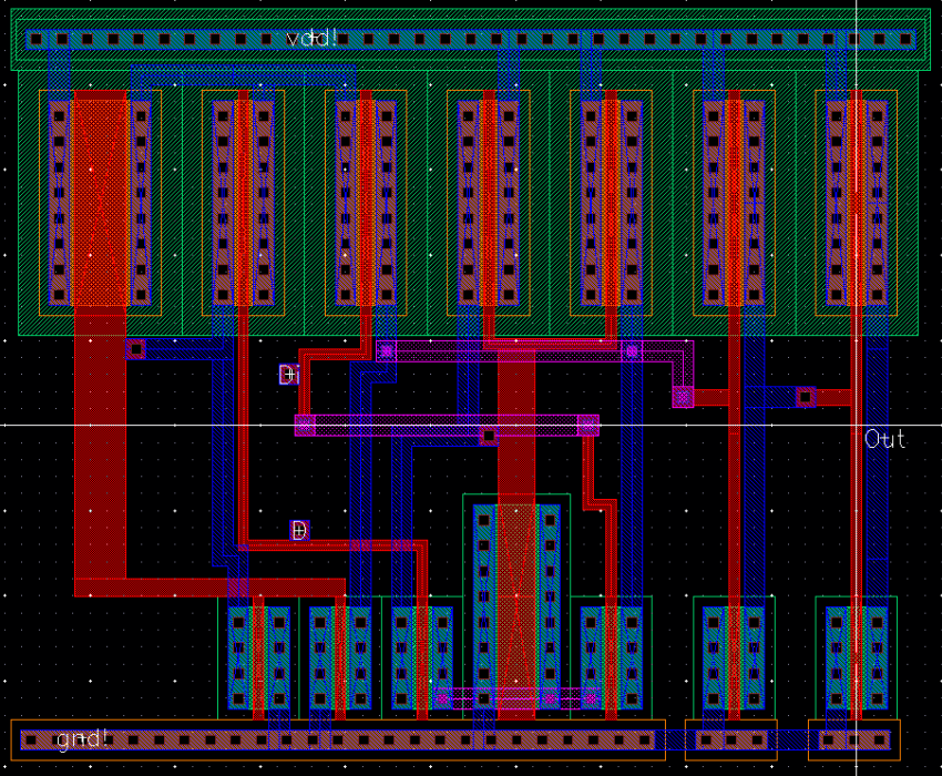
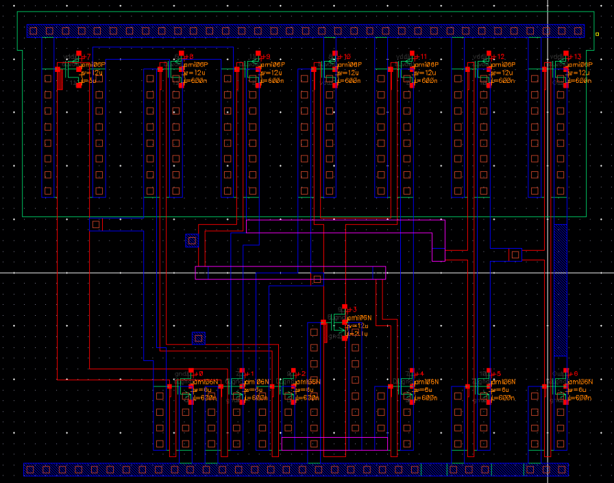
Layout of the design

Extracted view:

DRC & LVS passed:


My
layout design passes the DRC and LVS tests, so I believe that my design
and layout of the high-speed digital receiver was successful. This
concludes the final project for EE421L - Digital Integrated Circuit
Design Laboratory. I would like to thank Dr. Baker for his excellent
instruction and teaching methodology. Hopefully I can use the knowledge
I gained in the laboratory in my career in the near future.
Project Files:
labFinal_EE421L_WMW_f20.zip
Return to William Wherry Labs Directory