

Lab 5 - EE 421L Digital Integrated Circuit Design, Fall 2020
Design, layout, and simulation of a CMOS inverter.
Pre-lab work
Following Tutorial 3, we first create a schematic for the inverter using a 12u/0.6u PMOS in series with a 6u/0.6u NMOS. The pins of the inverter will be the input A and output Ai. We then make a symbol for the schematic.
Next, we have to make a layout that matches the schematic in order to pass the DRC and LVS checks. Following the instructions in Tutorial 3, we layout the MOSFETs similarly to the way we have in the past, but now the gates of the two MOSFETs are tied together with the poly layer (with a net which will be our input A) and the drain of the PMOS is tied to the source of the NMOS with a net that will be the output Ai. Then we DRC, extract the layout and check it with LVS.


Next, we simulate our schematic in order to compare it to our layout design. We set up a circuit like below using the symbol we created.


Using these settings in our circuit gives us a graph our input signal versus our output signals. As you can see our inverter appears to work.

Now we will change the settings so that our extracted layout is used for the simulation instead of the schematic view.


Comparing the graphs it appears that our layout functions identically to the schematic, which means our layout was successful.
Backing up our work:
As always we must backup our work. I backed up my work by downloading the lab files, zipping them up, and uploading them to my google drive.


With our layout completed, tested and our work backed up, the prelab is concluded.
Main lab content:
First, we have to make schematics and symbols for our two designs. Using the same process as Tutorial 3, we can make our 12u/6u inverter, which is just a 12u/0.6u PMOS in series with a 6u/0.6u NMOS. We can do the exact same thing again for the 48u/24u inverter, except we set the multiplier for each of these MOSFETs to M=4, so there are four of each in parallel, multiplying thewidths by four.


Next, we make a symbol for each of them. I used text boxes to label them for clarity.


Next we have to layout each inverter, DRC, then LVS them. First I did the 12u/6u, since it was exactly the same as the prelab.


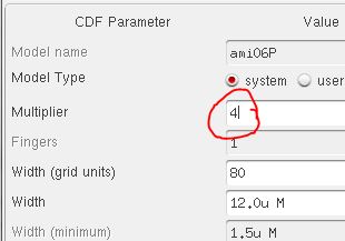
Next, laying out the 48u/24u inverter is a little more complicated. We want our PMOS and NMOS to have 4 fingers each, to multiply the width of the MOSFETs by 4. We do this by changing the "multiplier" setting when instantiating them from 1 to 4 as pictured.


After placing our PMOS and NMOS, we add the ntap and ptap respectively. We should make them kind of wide so they have good connections. We can do this by increasing the number of rows or columns as we like when we're instantiating them. You can see in the image below how our MOSFETs are much wider than usual due to the extra fingers.


Then we DRC, extract the layout and LVS the extracted layout versus the schematic that we made.


The design passed DRC and LVS, so now it is time to test both of the inverters in a circuit with capacitive loads to see how they function. We will be using 100fF, 1pF, 10pF and 100pF loads. First I will show the 48u/24u inverter schematic and simulations.

To simulate this circuit, we will use both SPICE and Ultrasim and compare the results. Ultrasim is usually used for larger circuits and trades speed for accuracy. The settings used for SPICE and Ultrasim are shown below.


On the top will be the SPICE results and on the bottom will be the Ultrasim results.
100fF Load:
SPICE:

Ultrasim:

1pF Load:
SPICE:

Ultrasim:

10pF Load:
SPICE:

Ultrasim:

100pF Load:
SPICE:

Ultrasim:

Since our circuit is not very complex, there is not much, if any, difference between the two simulators. If our circuit was more complex, it would probably be more advantageous to use Ultrasim over Spectre (SPICE) in our simulation, but for this lab either appears to be fine.
Next, we will do the same thing with the same loads for the 12u/6u inverter.

100fF Load:
SPICE:

Ultrasim:

1pF Load:
SPICE:

Ultrasim:

10pF Load:
SPICE:

Ultrasim:

100pF Load:
SPICE:

Ultrasim:

Conclusions:
Once again, since our circuits are not very complex, there is not much difference between Spectre (SPICE) and Ultrasim in our simulations. You can tell that the 48u/24u inverter has a better time dealing with high capacitance loads, but both seem to really struggle around the 10pF and higher mark. This is a good lesson that wider MOSFETs can handle higher capacitance loads. The biggest issue with the higher capacitances is that they take longer to charge and discharge, which means you get a poorly inverted or non-inverted signal at capacitances over 10pF with our designs. In digital logic this is unacceptable, because our high signal input would not become a low output signal or vice versa, which is the basic job of an inverter.
For comparison of the two inverters, I did a parametric analysis to show all of our different capacitance loads in one graph so you can really see the difference.
12u/6u:

48u/24u:

Download for all of this lab's work:
Backing up our work:
As always we must back up our work. I back up my work by downloading the lab directory, zipping it up, and uploading it to my google drive.


With our inverters completed, tested and backed up, lab 5 is concluded.
Return to William Wherry Labs Directory