Lab 4 - EE 421L Digital Integrated Circuit Design, Fall 2020
Author: William Wherry
Email: wherrw1@unlv.nevada.edu9/16/2020
IV characteristics and layout of NMOS and PMOS devices in ON's C5 process
Pre-lab work:
- Back-up all of your work from the lab and the course.
- Read through this lab before starting it.
- Go through Tutorial 2 seen here.
- In
the simulations in this lab the body of all NMOS devices (the
substrate) should be at ground (gnd!) and the body of all PMOS devices
(the n-well) should be at a vdd! of 5V.
Following the instructions of Tutorial 2, the first thing we do is create a NMOS schematic and symbol.


Next, we make a circuit to test our NMOS schematic and use parametric analysis in the ADE.


Now
we will make a layout design of this NMOS and then test it again.
First, we follow the guidelines of Tutorial 2 to layout the design. At
the end of the tutorial we get a design like the one below. We then DRC
it, Extract it, and perform the LVS.


Now
it is ready to be tested in the same manner as the schematic. If it
works we will get similar results. Following tutorial 2 instructions,
we have to be sure that the extracted layout is simulated, rather than
the schematic. We do this by inserting "extracted" before "schematic"
in the environment options in the ADE.

As you can see, our extracted layout performs similarly to the schematic.
Next, we will do the same procedure, but with a PMOS. First we create a PMOS schematic and symbol.


Then
we simulate it the same way, keeping in mind that PMOS body needs to be
at VDD, rather than gnd like the NMOS.


Now
we layout the PMOS by following Tutorial 2. At the end we come out with
a schematic that looks like the image below. We then DRC, extract it,
and perform the LVS function.


Now
we perform a parametric analysis using the same method as the NMOS,
making sure that we add the word "extracted" before "schematic" in the
environment options of the ADE.
Once again, our layout works similarly to the schematic simulation.
Backing up work:
As
always, we must back up our work when we are done. I back up my work by
downloading the Tutorial 2 library folder that I was working in and
email it to myself.


With Tutorial 2 complete and backed up, the prelab is concluded.
Main Lab Content:
- Generate 4 schematics and simulations (see the examples in the Ch6_IC61 library, but note that for the PMOS body should be at vdd! instead of gnd!):
- A schematic for simulating ID
v. VDS of an NMOS device for VGS varying from 0 to 5 V in 1 V steps
while VDS varies from 0 to 5 V in 1 mV steps. Use a 6u/600n
width-to-length ratio.
- A
schematic for simulating ID v. VGS of an NMOS device for VDS = 100 mV
where VGS varies from 0 to 2 V in 1 mV steps. Again use a 6u/600n
width-to-length ratio.
- A
schematic for simulating ID v. VSD (note VSD not VDS) of a PMOS device
for VSG (not VGS) varying from 0 to 5 V in 1 V steps while VSD varies
from 0 to 5 V in 1 mV steps. Use a 12u/600n width-to-length ratio.
- A
schematic for simulating ID v. VSG of a PMOS device for VSD = 100 mV
where VSG varies from 0 to 2 V in 1 mV steps. Again, use a 12u/600n
width-to-length ratio.
- Lay
out a 6u/0.6u NMOS device and connect all 4 MOSFET terminals to probe
pads (which can be considerably smaller than bond pads [see MOSIS design rules] and directly adjacent to the MOSFET (so the layout is relative small).
- Show your layout passes DRCs.
- Make a corresponding schematic so you can LVS your layout.
- Lay out a 12u/0.6u PMOS device and connect all 4 MOSFET terminals to probe pads.
- Show your layout passes DRCs.
- Make a corresponding schematic so you can LVS your layout.
ID v. VDS of an NMOS (6u/600n):
Similarly
to Tutorial 2, I put together a circuit using my symbol that I created
from tutorial 2, since it was already designed at 6u/600n
width-to-length ratio.

We
are going to use parametric analysis to sweep VGS from 0 to 5V, while
we sweep VDS from 0 to 5V in 1mV steps. This should result in a graph
that shows us ID vs VDS in our NMOS. The settings to perform this
analysis are shown below.


You can see that our graph is similar to the ones we did in Tutorial 2 in the prelab section.
ID v. VGS of an NMOS (6u/600n):
Using the same circuit as ID v. VDS, we can simply change the value of VDS to 100mV, but now we are sweeping VGS from 0 to 2V.

We
have to change the dc sweep to the VGS input and also change the values
from 0 to 2V. We don't perform a parametric analysis here, only a
regular simulation. Below are the settings and results.


These results show Id v. VGS in our NMOS circuit.
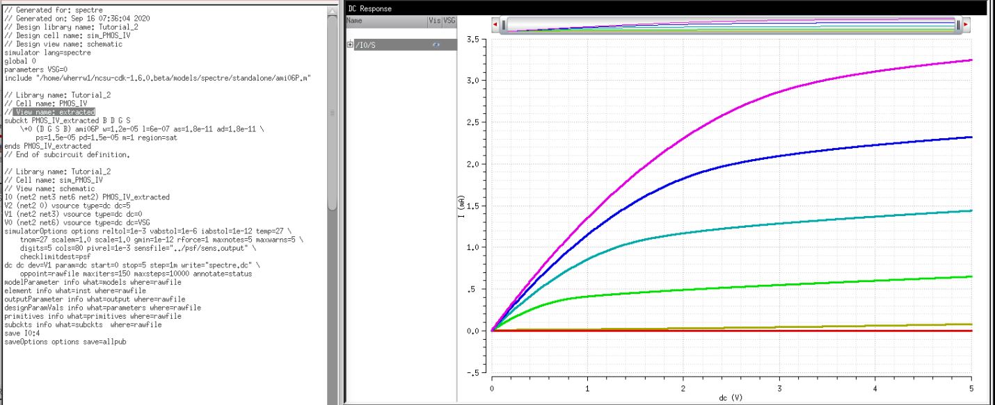
Id v. VSD (Note VSD, not VDS) of a PMOS (12u/600n):
We
can perform the Id v. VSD analysis basically the same way we did in
Tutorial 2. I will once again be using my PMOS I designed following
that tutorial and use it to implement the circuit below.

We
set up the ADE with parametric analysis similarly to the NMOS, but this
time we will be sweeping VSG from 0 to 5V in 1V steps, while we also
sweep VSD from 0 to 5V in 1mV steps. This will allow us to graph Id v.
VSD. The settings I used to perform this analysis and the results are
below.


The results are similar to the results we got in the prelab.
Id v. VSG of a PMOS (12u/600n):
For
this circuit we have to change VSD to 100mV and sweep VSG from 0 to 2V
in 1mV steps. We do this the same way as the NMOS, but using the
circuit we made for the PMOS. The setup for the circuit is below.

The
settings are a little different than the previous PMOS circuit's
settings. We have to change the dc sweep from VSD over to VSG and sweep
it from 0 to 2V now. We also don't need to use parametric analysis for
this one. The settings and results are pictured below.


As you can see we have a graph of Id v. VSG resulting from our change of settings.
Lay out a 6u/0.6u NMOS device and connect all 4 MOSFET terminals to probe pads:
Since we are required to layout a 6u/0.6u NMOS, I decided to just use
our prelab NMOS layout as a base structure. To do this, I simply copied
my NMOS files over to the lab4 library and renamed them. There was a
problem with this idea though, as the Tutorial 2 had use make the body
terminal of our NMOS into gnd, but I needed it to be "B" for body now.
So, I simply went into the layout, deleted the gnd pin net, and
replaced it with a "B" output pin. I then went and updated the
schematic to have a "B" output pin so they match. I DRC'd the changes
and no errors were reported.
In
order to add probe pads to my layout, I had to consider the metal
layers. The probe pads are made of Metal 3 and Glass layers. Metal 3 is
the highest layer and can't be reached from Metal 1. There needs to be
an intermediate Metal 2 layer connecting them. Therefore, I had to
expand the Metal 1 layers connected to the NMOS drain, source, gate,
and body terminals, connect them to a Metal 2 layer with M1_M2
connectors, then connect the Metal 2 layer to Metal 3 with M2_M3
connectors in order to get to the probe pads. You can see the base NMOS
I used below, then the changes I made to get the results of what I just
explained.
Base NMOS (before gnd was changed to "B" pin):

Metal layers added to get to the probe pads (also with gnd changed to "B" pin added):

Next,
I had to connect those Metal 3 layers to the probe pads, but you have
to make them at least 30um away from the nearest metal layer or you'll
get an error when you try to DRC.

The full view of my finished layout:


The
DRC shows no errors, so the layout seems to be fine for now. In order
to perform the LVS, we also need a schematic. Below are the schematic
and symbol I came up with.


These
are different than the prelab ones we made, since the NMOS doesn't
automatically put the body at gnd anymore, but instead to a pin. Now we
can extract the layout and try to perform the LVS.


The
extracted layout and schematic seem to pass the LVS check just fine, so
now it is time to move on to the next part of the lab.
Lay out a 12u/0.6u PMOS device and connect all 4 MOSFET terminals to probe pads:
Once
again, since we made a 12u/600n PMOS in Tutorial 2 in the prelab, I
simply copied over the files into my lab 4 library and modified the
layout and schematic. I started with the base PMOS layout and added
Metal layers the same way as the NMOS in order to connect to the probe
pads later. I had to do it the same way; Metal 1 to Metal 2 to Metal 3
using instances of the M1_M2 and M2_M3 connectors. The results of
making these connections are below.
Base PMOS layout before adding connections:

After adding connections:

Just
as with the NMOS, in order to add probe pads to the layout without
getting errors, they must be at least 30um away from the nearest metal
layer.

Full view of finished layout:
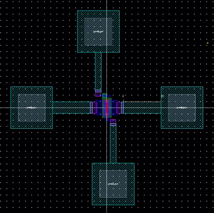

The
full layout passes the DRC, so we are successful for now. Next we need
a schematic in order to perform a LVS test. The schematic and symbol I
made are shown below.
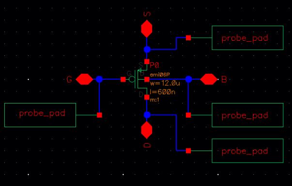

Now we can perform a LVS test on the schematic vs the extracted layout.


The designs passed the LVS test, so it appears we are successful!
Backing up our work:
We
must always back up our work just in case. The way I back up my work is
by zipping up the directory and emailing it to myself as shown below.


With our designs laid out, tested, and backed up, lab 4 is concluded.
Return to William Wherry Labs Directory