

Lab 3 - EE 421L Digital Integrated Circuit Design, Fall 2020
This lab will focus on the layout of the 10-bit DAC you designed and simulated in Lab 2
Prelab Work:
As always, we backup our previous work just in case.
Tutorial 1 involves designing a schematic for a simple voltage divider using two 10k-resistors. We have to not only create the schematic for that voltage divider, but also create a symbol and layout for it, so it could theoretically be manufactured. First, we create a schematic for the voltage divider.

Then we create a symbol for it.

Then we have to make a layout for it, which is the technical file that could be used to manufacture the component. We made a 10k resistor layout earlier in the tutorial that we will simply use as an instance twice. We calculated that the resistor would need to be of 4.5u width and 56.1u long in order to achieve about 10k ohms resistance with a sheet resistance of ~800 ohms per square. If we divide 56.1 by 4.5 we can see that 56.1/4.5 = 12.47squares * 800 = ~9,975 ohms. Keep in mind that the DRC file checks if the dimensions are divisible by 0.15 because that is what is required by the process we are using. 56.1/.15 = 374 and 4.5/.15 = 30, so our DRC should give us no problems. Laying out our resistor looks like this:

We check the DRC for errors, then verify-> extract, then check our extracted resistor for the value of resistance Cadence has calculated.

As you can see, our resistor came out pretty close to 10k ohms at 10.21k ohms. We can now use this resistor we created as an instance in our voltage divider for tutorial 1 as seen below.

We
connect the resistor pins with Metal 1 and create pins with the same
names as our voltage divider symbol and schematic. We can then check
the DRC again, extract this layout, then check the LVS against the
schematic to see if they match up. With our 10k resistor and voltage
divider successfully created and backed up, prelab 3 is concluded.
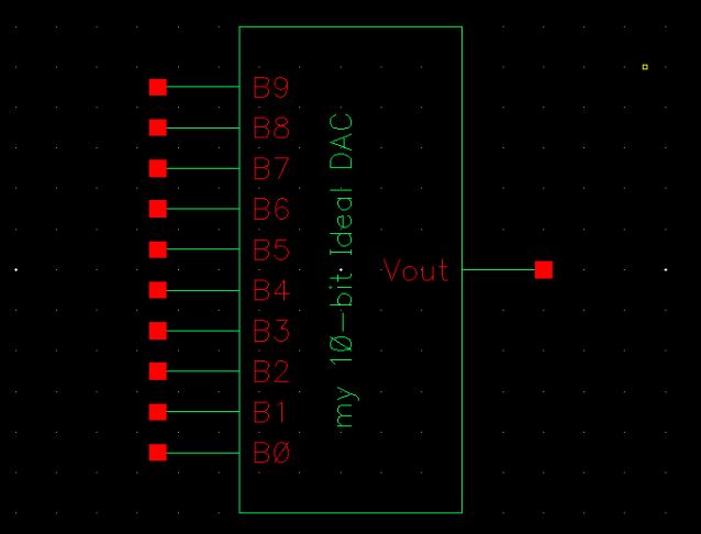
To begin with, we have our schematic and symbol of our 10-bit DAC from lab 2.
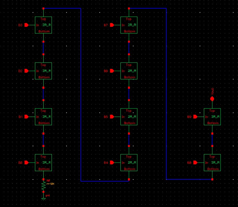
Now we will design a layout using the 10k resistor layout from Tutorial 1. We could just place a whole bunch of instances of the 10k resistor, but a more efficient way is to create a layout for the 2R_R symbol used in the DAC schematic. That way we can place ten 2R_R instances rather than try to evenly space out 30 10k resistors. We create the layout, then DRC check it, then extract the layout, then LVS it to make sure it matches up. Once that is done we can instantiate it in our DAC schematic.


Now we create a layout for the 10-bit DAC and begin placing instances of our 2R_R layout. We can connect the "Top" and "Bottom" pins using Metal 1, which is a requirement of lab 3. We can then add the corresponding pins that we require (making sure their names match the 10-bit DAC schematic and symbol pin names) by selecting metal 1 and creating input or output pins as needed.

You can see in the area surrounded by the yellow square that our layout we created for 2R_R has allowed us to efficiently place our resistors in a uniform fashion. This not only saves time in the long run, but allows for more symmetrical designs and less sloppy work. Now we continue placing instances of 2R_R until our layout is complete.


As always we must back up our work. I back up my work by downloading the lab design directory as well as the webpage files, zip them up and email them to myself.


With our 10-bit DAC layout completed and our work backed up, lab 3 is concluded.
Return to William Wherry Labs Directory