Lab 8- EE 421L Fall 2020 

Authored by: Nathan Pina, Quinton Micheau, Gabriel Gabonia
Email: pinan1@unlv.nevada.edu, micheauq@unlv.nevada.edu, gabonia@unlv.nevada.edu
Due Date: 12/02/20


Lab description:

Generating a test chip layout for submission to MOSIS for fabrication 

Pre-Lab:

- Back-up all of your work from the lab and the course.
- Go through Cadence Tutorial 6 seen here.


Tutorial 6 goes through the process of designing and laying out a padframe for fabrication.

fig5.JPG

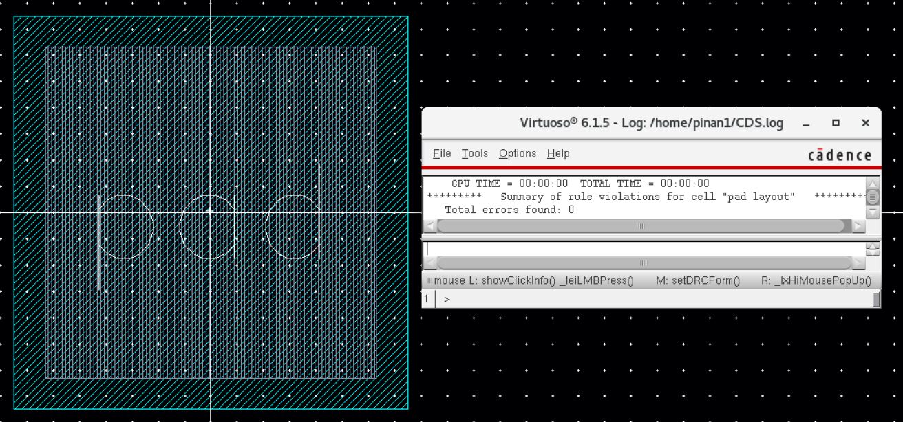
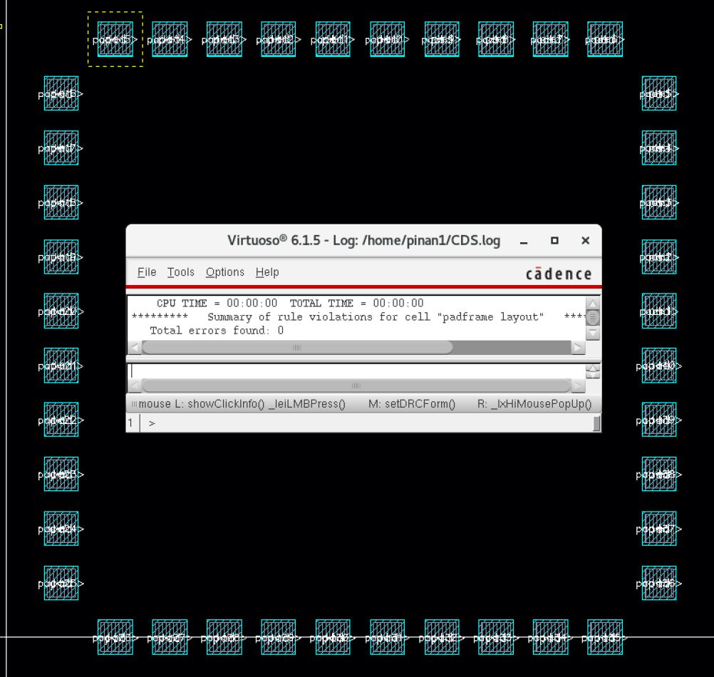
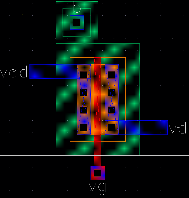
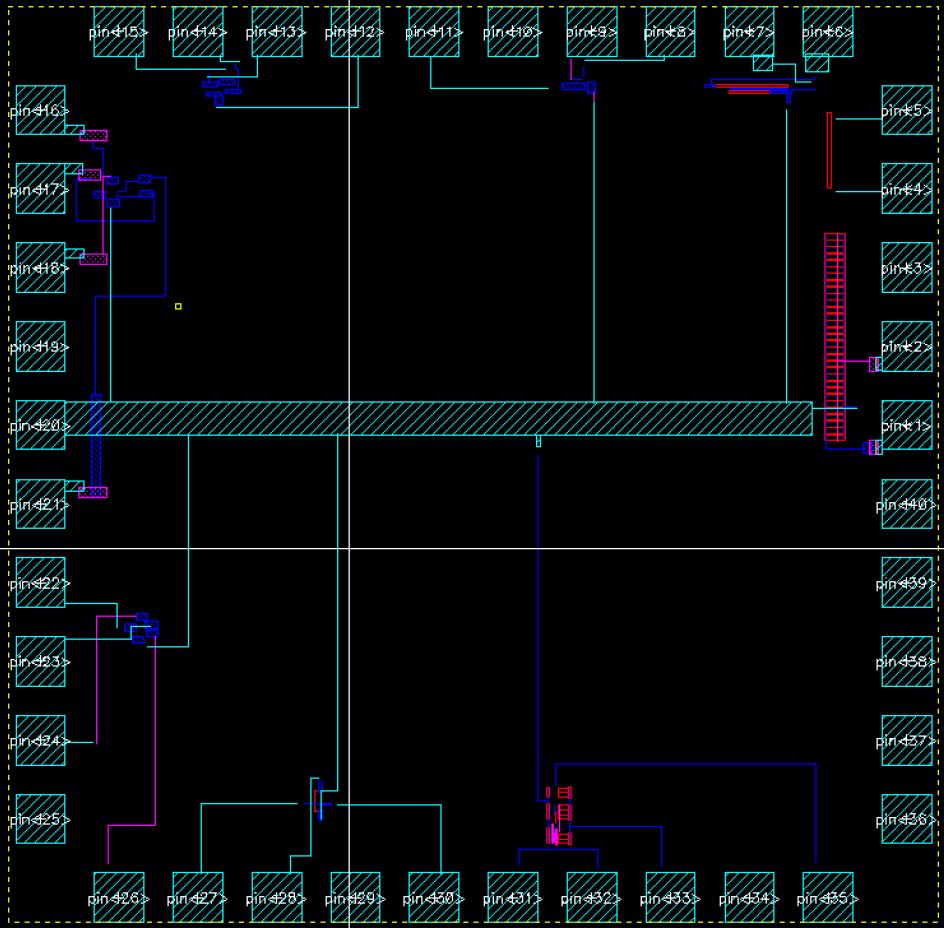
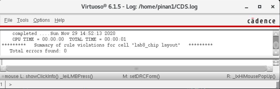
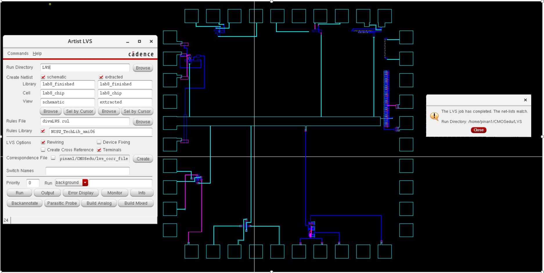
Layout of Pad w/DRC check

fig6.JPG

Layout of Padframe w/DRC check

fig8.JPG

Symbol of Padframe

Main Lab Work:

This lab will involve the design and layout of a chip containing the test structures of various circuits we have done throughout the semester. Each of these test circuits will have its own power while the ground will be shared between the circuits.

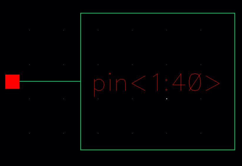
Additonally, pin 20 will be ground.

The following test structures will be included:

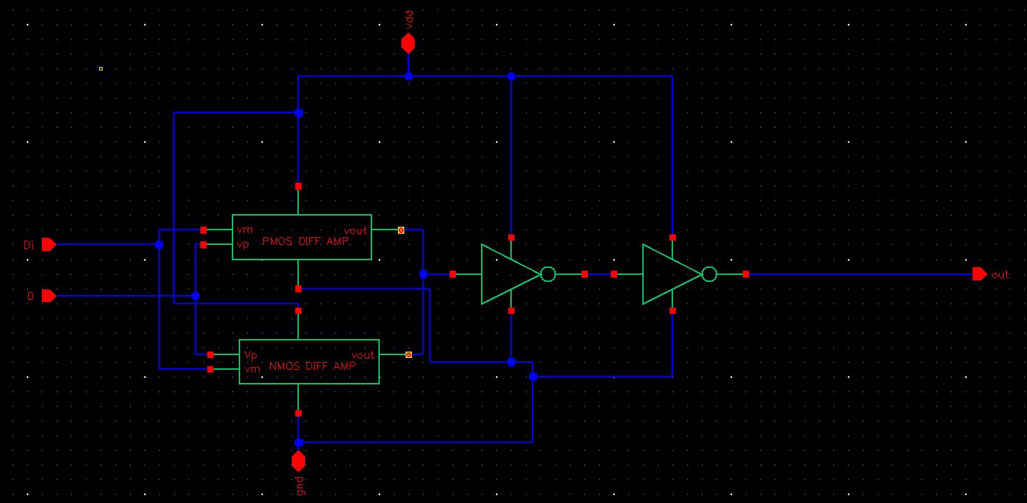
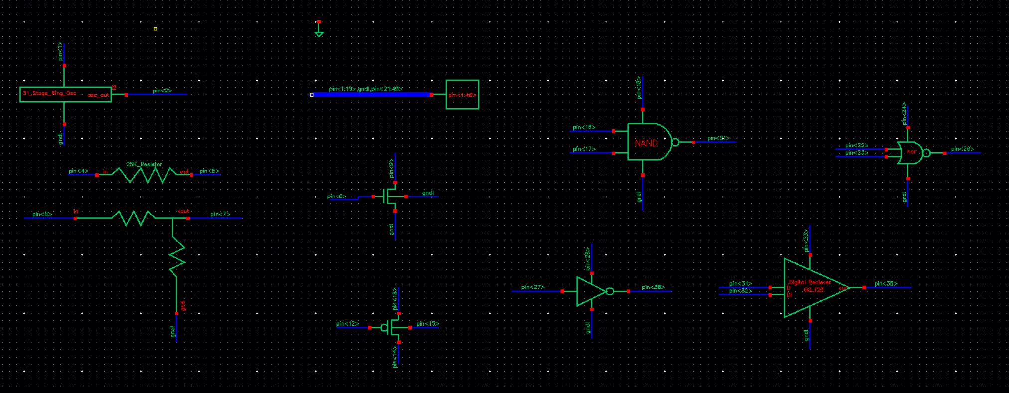
- One or more course projects (Digital Reciever)

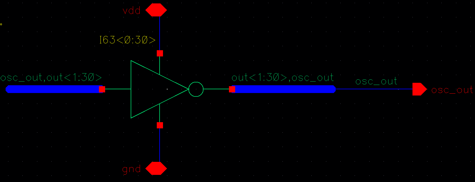
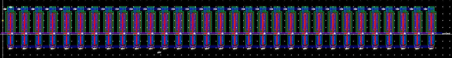
- 31-stage ring oscillator with a buffer for driving a 20pF off-chip load

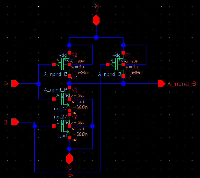
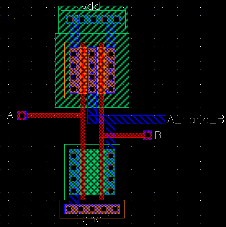
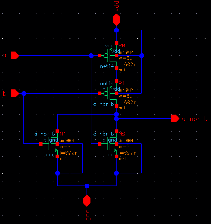
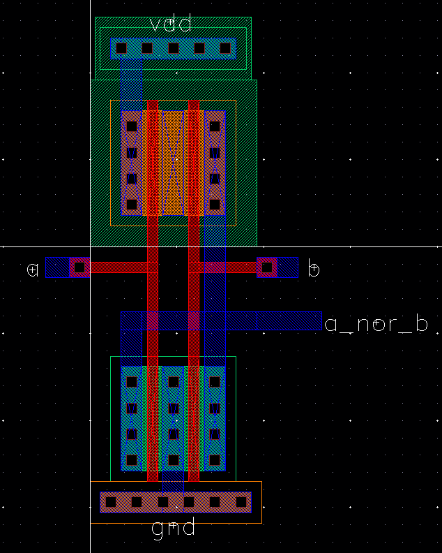
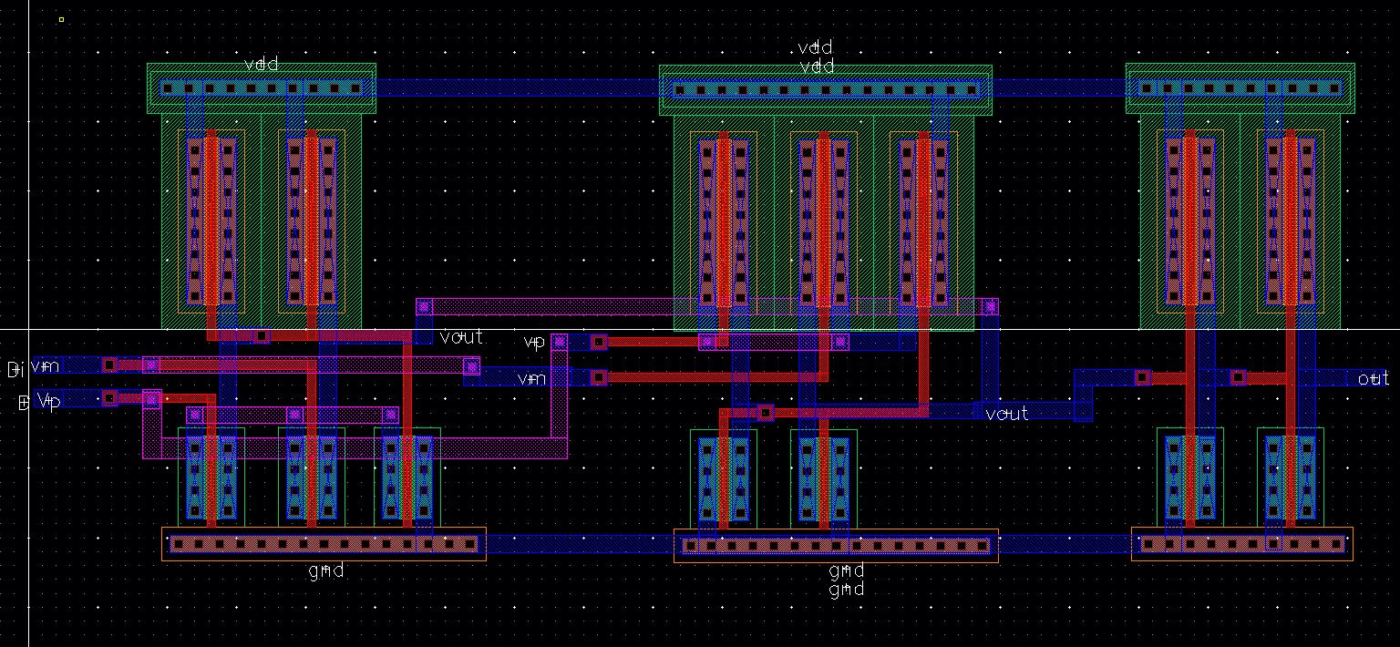
- NAND and NOR gates using 6/0.6 NMOSs and PMOSs

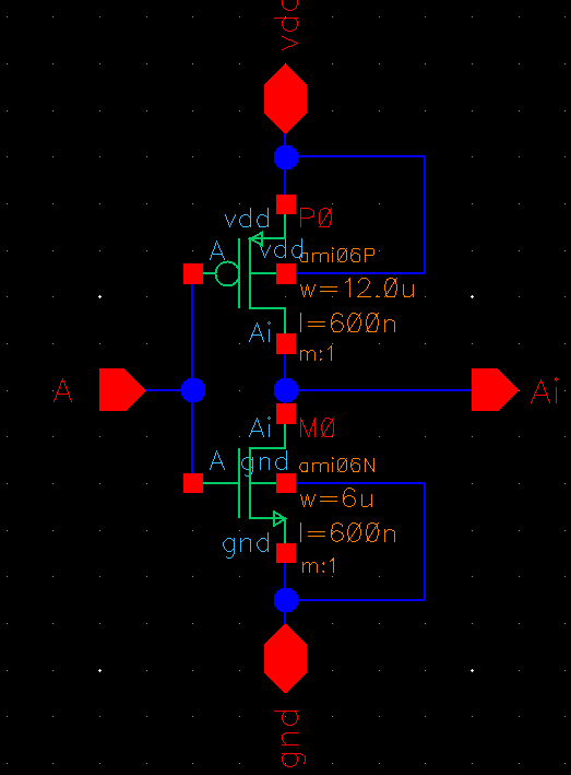
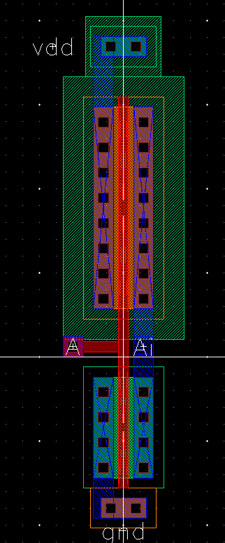
- Inverter made with a 6/0.6 NMOS and a 12/0.6 PMOS

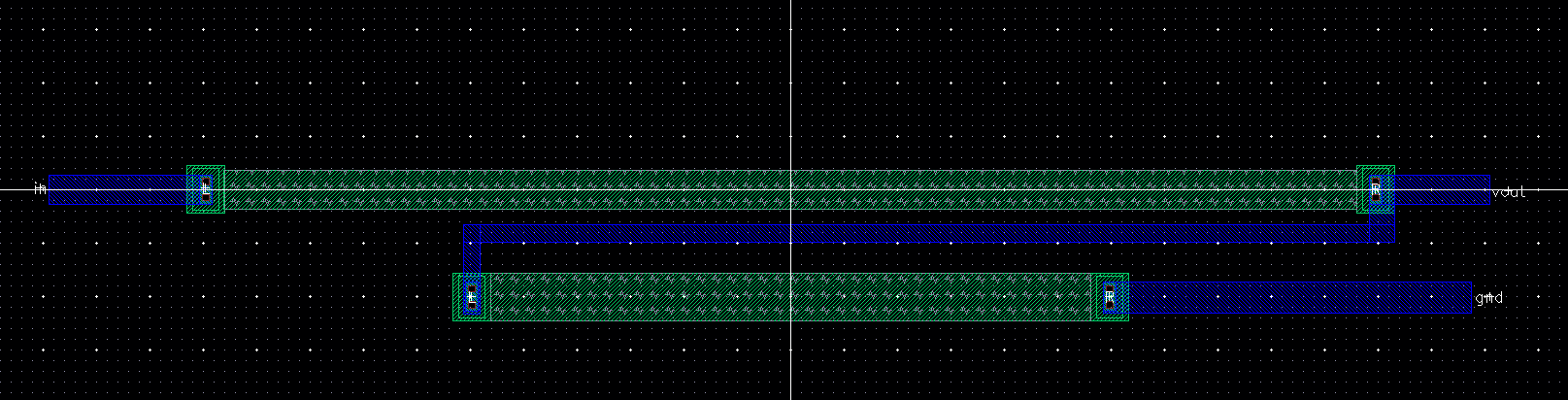
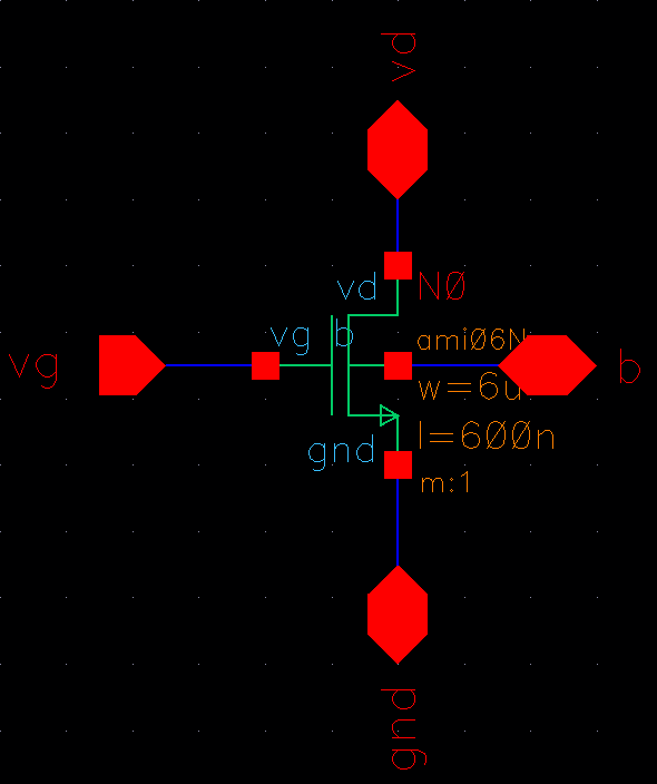
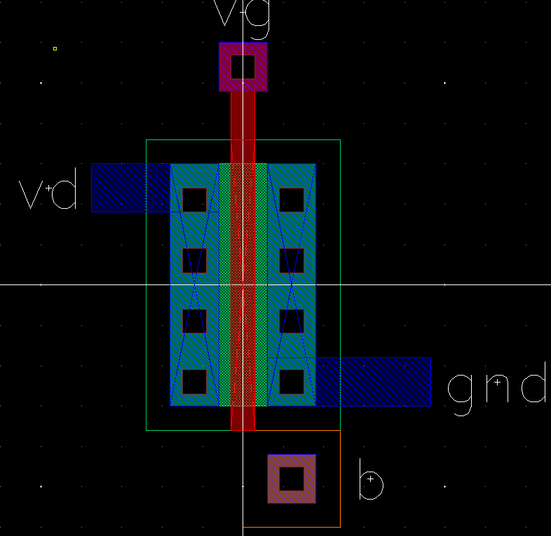
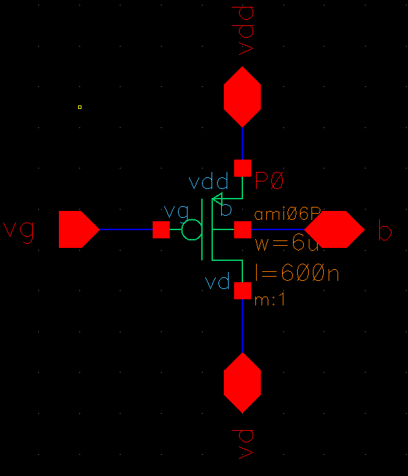
- Transistors, both PMOS and NMOS, measuring 6u/0.6u where all 4 terminals of each device are connected to bond pads

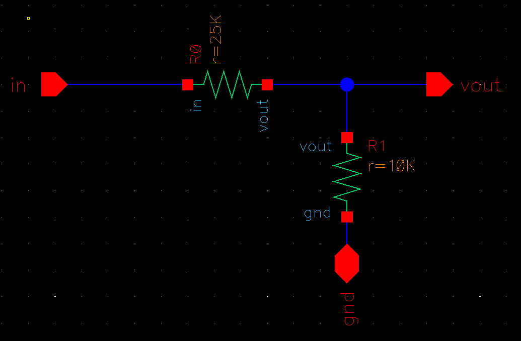
- 25k/10k voltage divider
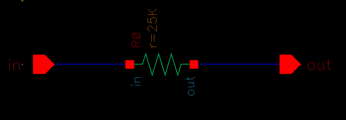
- 25k n-well resistor

31-State Ring Oscillator (Schemaitc/Layout)

ring_osc_schematic.PNGring_osc_layout.PNG

ConnectionsPin Names
  • vdd
  • gnd
  • osc_out
  • 1
  • gnd!/20
  •  2

25k Resistor (Schemaitc/Layout)

resistor_schematic.PNG resistor_layout.PNG

ConnectionsPin Names
  • in
  • out
  • 4
  • 5

10k/25k Voltage Divider (Schemaitc/Layout)

voltage_divider_schematic.PNGvoltage_divider_layout.PNG

ConnectionsPin Names
  • in
  • vout
  • gnd
  • 6
  • 7
  • gnd!/20


NMOS (Schemaitc/Layout)

nmos_schematic.PNGnmos_layout.PNG

ConnectionsPin Names
  • vg
  • vd
  • b
  • gnd
  • 8
  • 9
  • gnd!/20
  • gnd!/20

PMOS (Schemaitc/Layout)
pmos_schematic.PNGpmos_layout.PNG

ConnectionsPin Names
  • vg
  • vdd
  • vd
  • b
  • 12
  • 13
  • 14
  • 15


NAND Gate (Schemaitc/Layout)

nand_schematic.PNGnand_layout.PNG

ConnectionsPin Names
  • A
  • B
  • vdd
  • A_nand_B
  • gnd
  • 16
  • 17
  • 18
  • 21
  • gnd!/20

NOR Gate (Schemaitc/Layout)

nor_schematic.PNGnor_layout.PNG

ConnectionsPin Names
  • a
  • b
  • vdd
  • a_nor_b
  • gnd
  • 22
  • 23
  • 24
  • 26
  • gnd!/20


Inverter (Schemaitc/Layout)

inverter_schematic.PNGinverter_layout.PNG

ConnectionsPin Names
  • A
  • vdd
  • Ai
  • gnd
  • 27
  • 28
  • 30
  • gnd!/20


Digital Reciever (Schemaitc/Layout)

digital_reciever_schematic.JPGdigital_reciever_layout.JPG

ConnectionsPin Names
  • D
  • Di
  • vdd
  • out
  • gnd
  • 31
  • 32
  • 33
  • 35
  • gnd!/20

Padframe - Fully Built (Schemaitc/Layout/Symbol)

fig1.JPG

Schematic for Padframe


fig8.JPG
Symbol for Padframe

fig3.JPGfig2.JPG
Layout
for Padframe w/DRC Check

fig10.JPG

Extracted View of Padframe w/LVS Check

Completed Directory: lab8.zip

Lab Backup
After I completed this lab, I made sure to back up all files (schematics, simulations, screenshots etc.) into a zip file and upload to my Google Drive

fig11.JPG