Lab 7 - EE 421L
Authored
by Michael Nguyen
Email: nguyem9@unlv.nevada.edu
11/18/2020
Pre-lab work
- Back-up all of your work from the lab and the course.
- Go through Tutorial 5 seen here.
- Read through the entire lab before starting it.
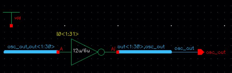
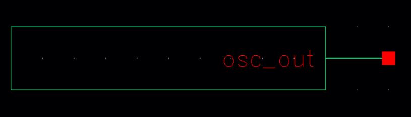
Ring
Oscillator Schematic
Symbol
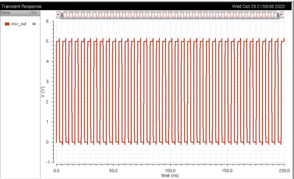
Simulation
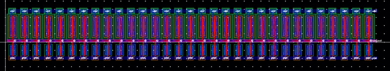
Layout
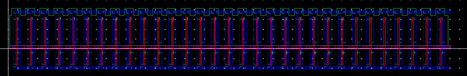
Extracted

DRC
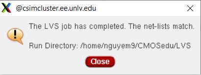
LVS __________________________________________________________________________________________________________________________
Laboratory Procedure
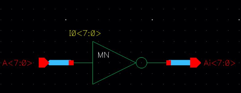
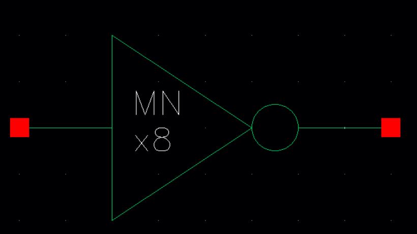
1. 4-bit Inverter


Transistor Level
Symbol

Schematic


Simulation
Schematic
Simulation
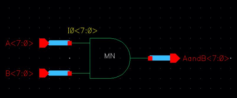
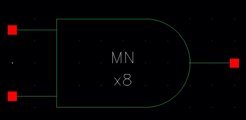
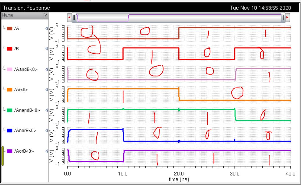
2. 2-input 8-bit Gates and 8-bit Inverter
Transistor Level


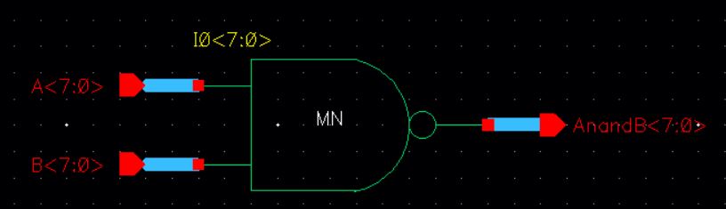
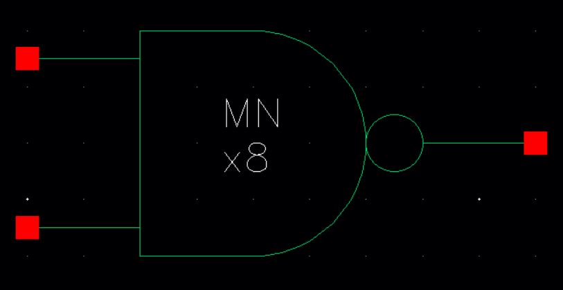
NAND
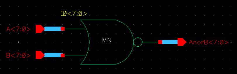
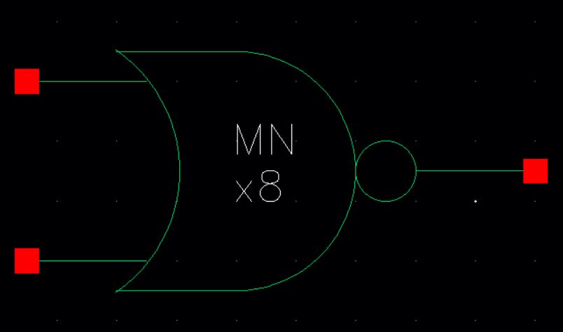
NOR
For
efficiency instead of building the AND and OR gates in transistor
level, it's easier to get rid of the NOT in NAND and NOR by adding an
inverter to the output

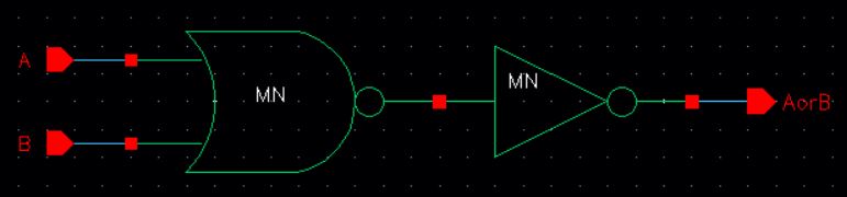
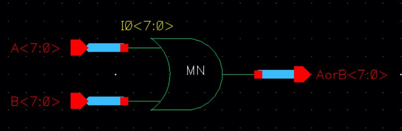
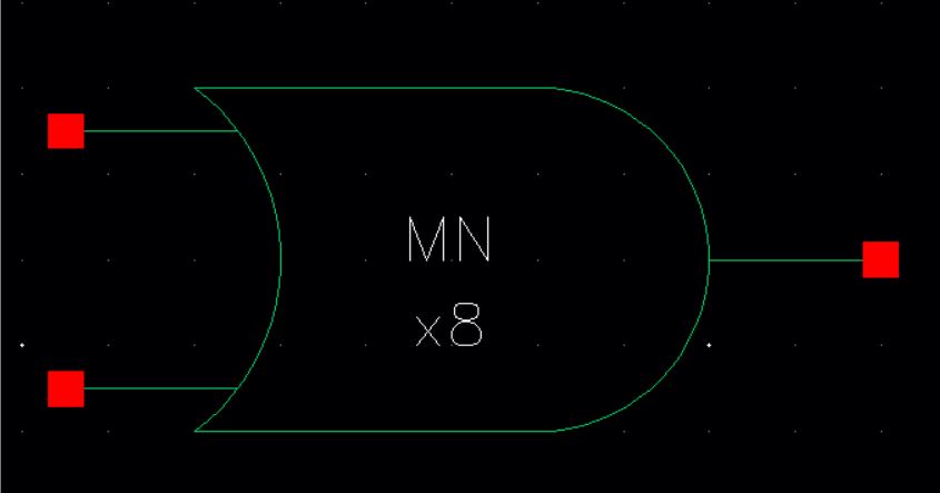
AND
OR
Gates
Schematic
Symbol
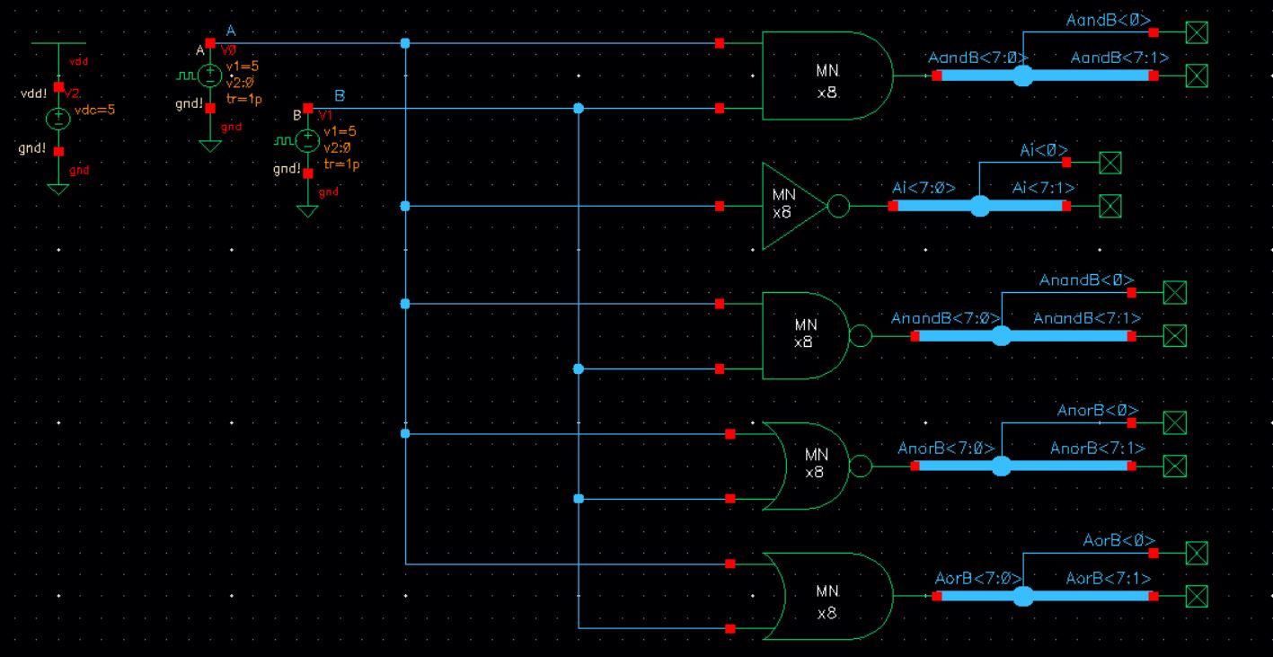
Schematic
Simulation
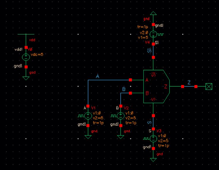
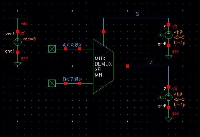
3. MUX/DEMUX
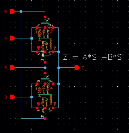
Pure MUX
MUX/DEMUX
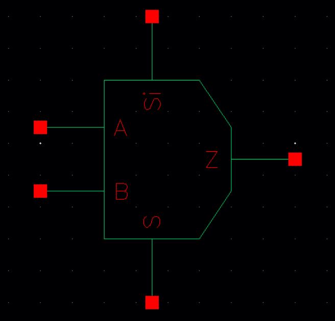
Symbol
Pure MUX A and B are input and Z is output, MUX/DEMUX A,B, and Z are input/output.
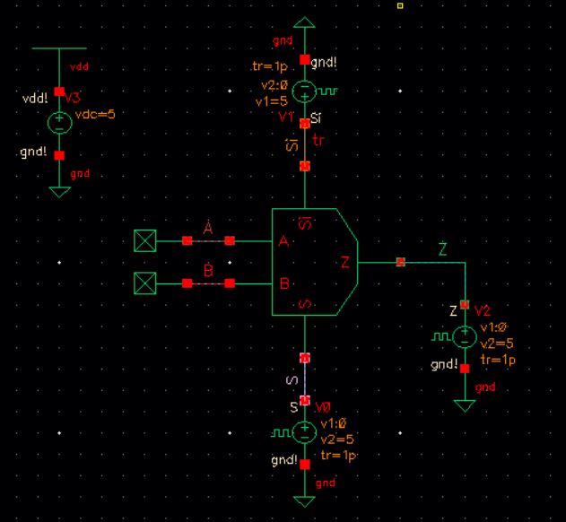
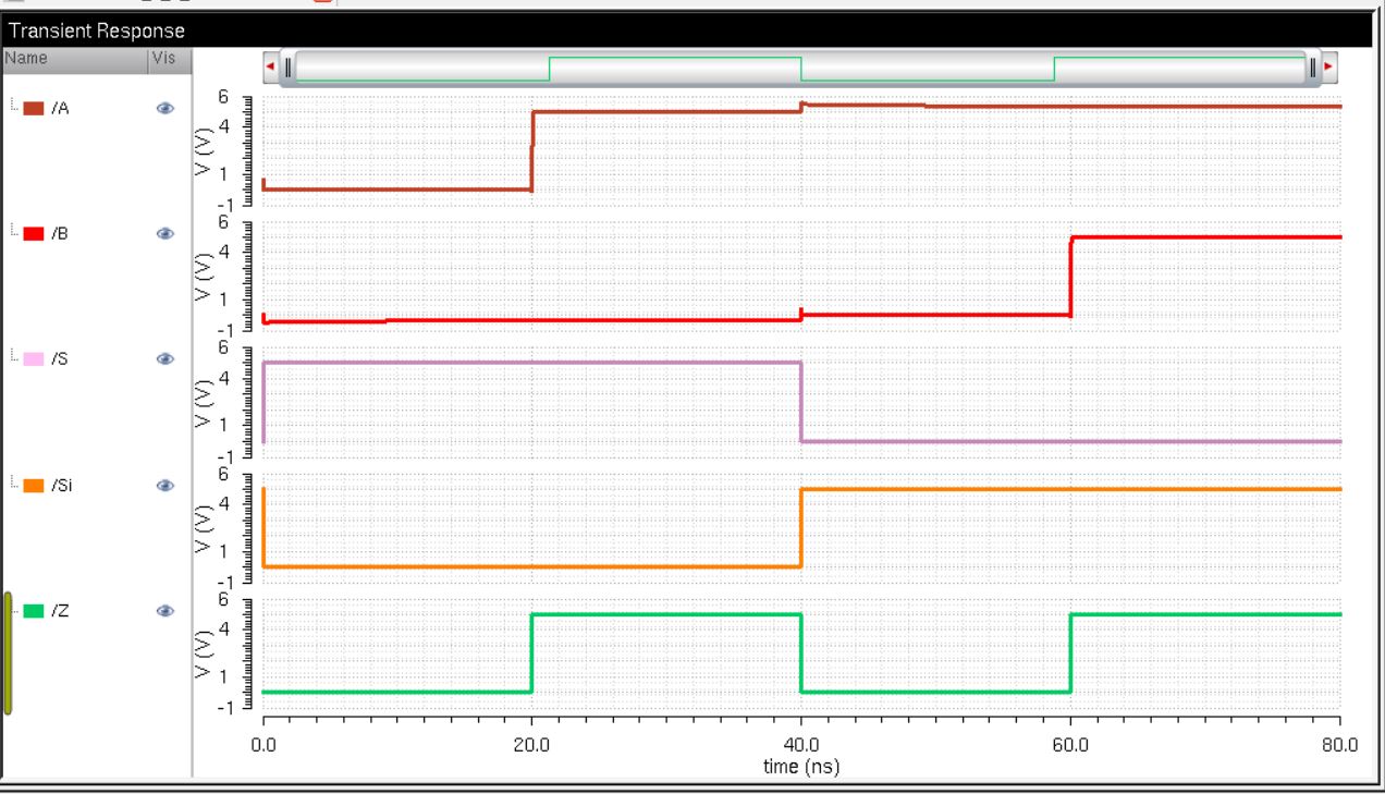
i. 2-input Select
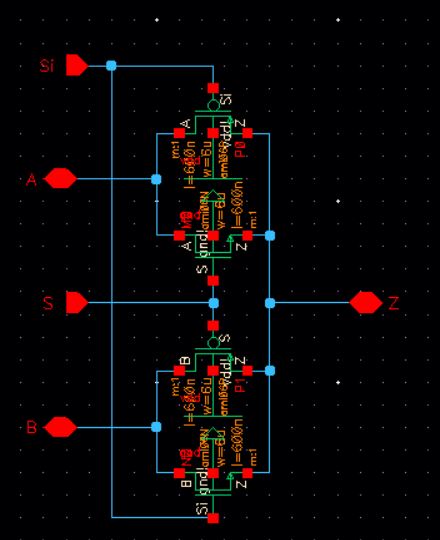
MUX
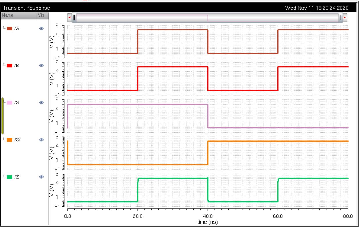
MUX S is high A propogates through, Si is high B propogates through.
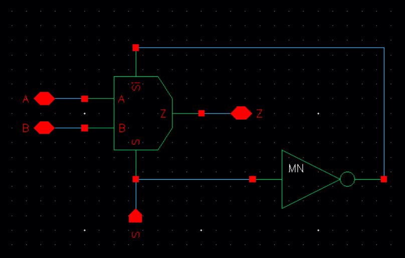
DEMUX
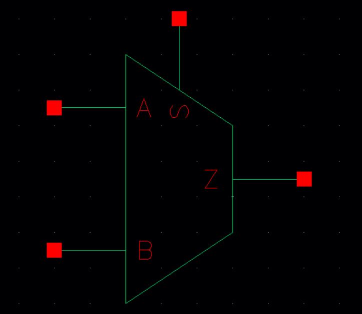
ii. Single Input Select
Schematic
Symbol
The single select MUX/DEMUX behaves roughly like the 2 input select MUX/DEMUX above.
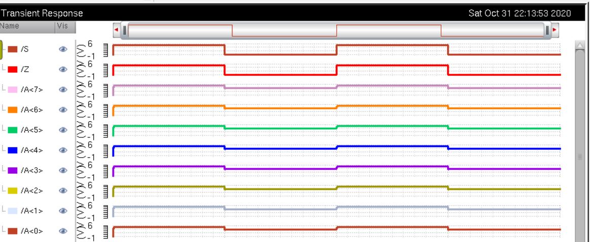
iii. 8-bit MUX/DEMUX
MUX 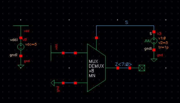
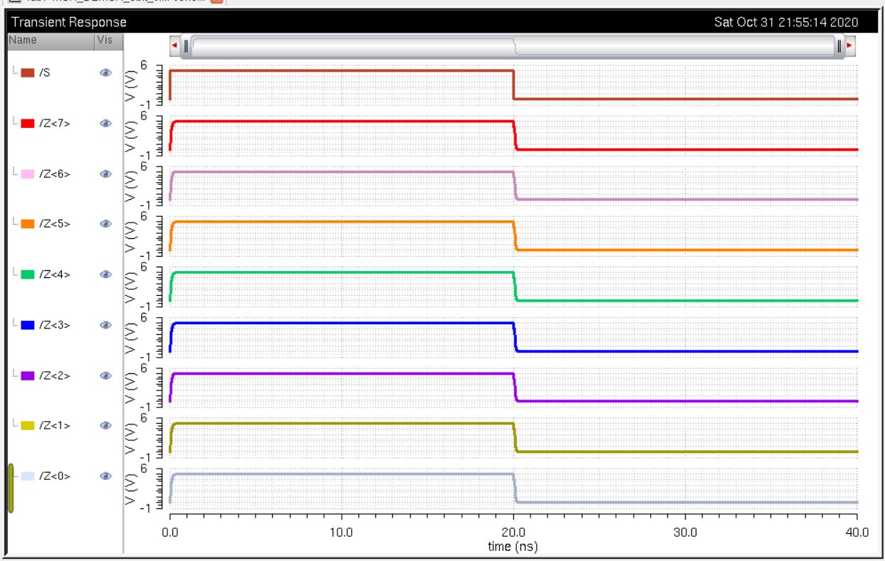
DEMUX
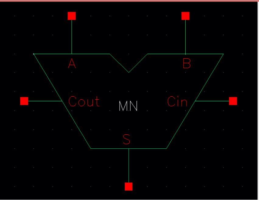
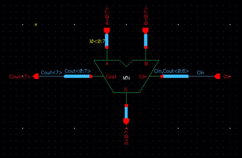
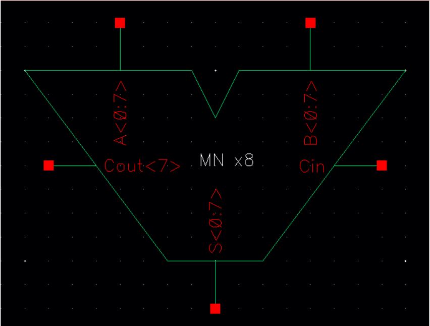
4. AOI FULL ADDER
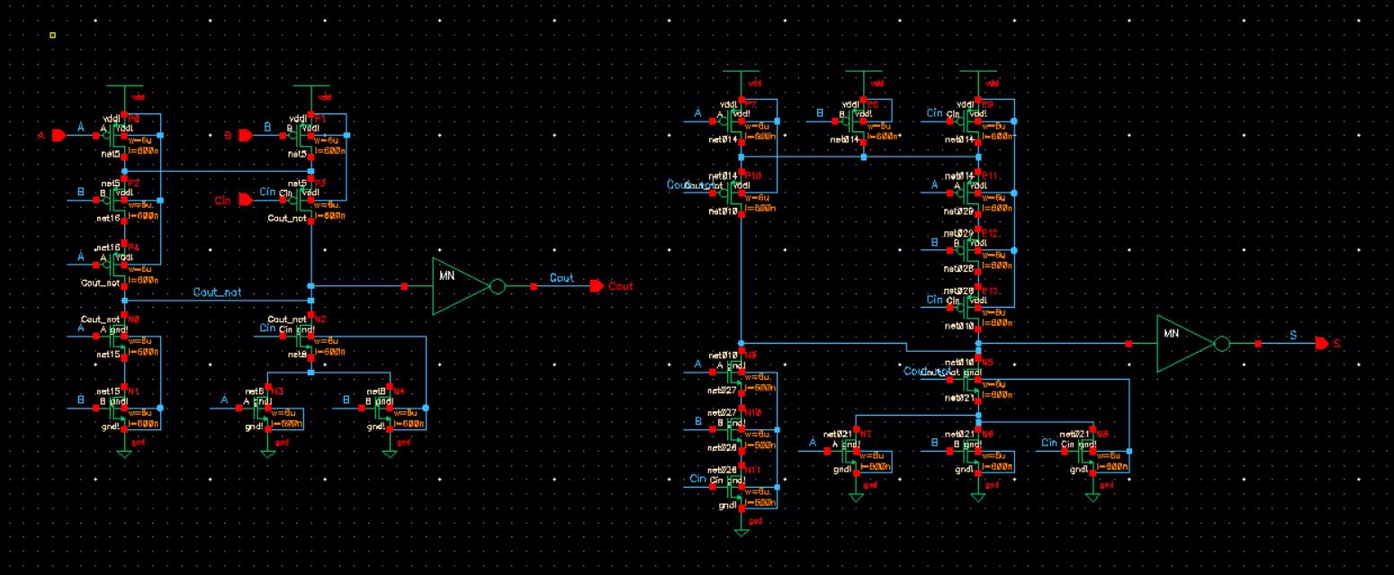
Schematic
Symbol
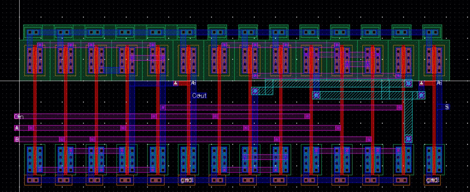
Layout
Extracted

DRC
LVS
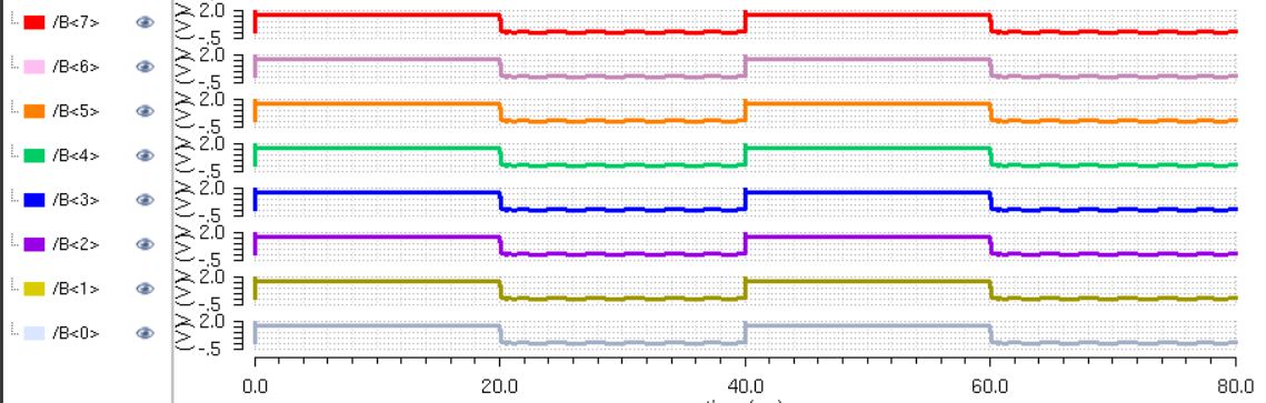
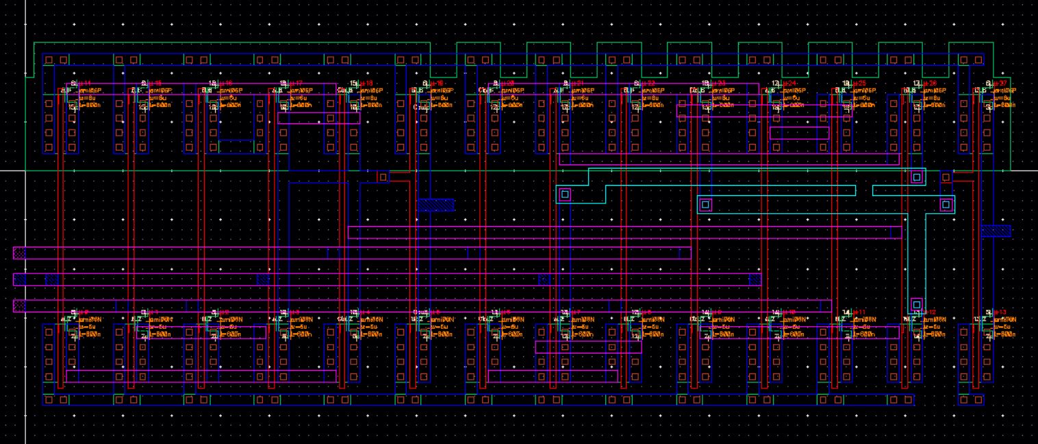
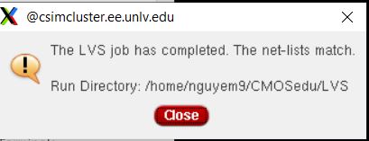
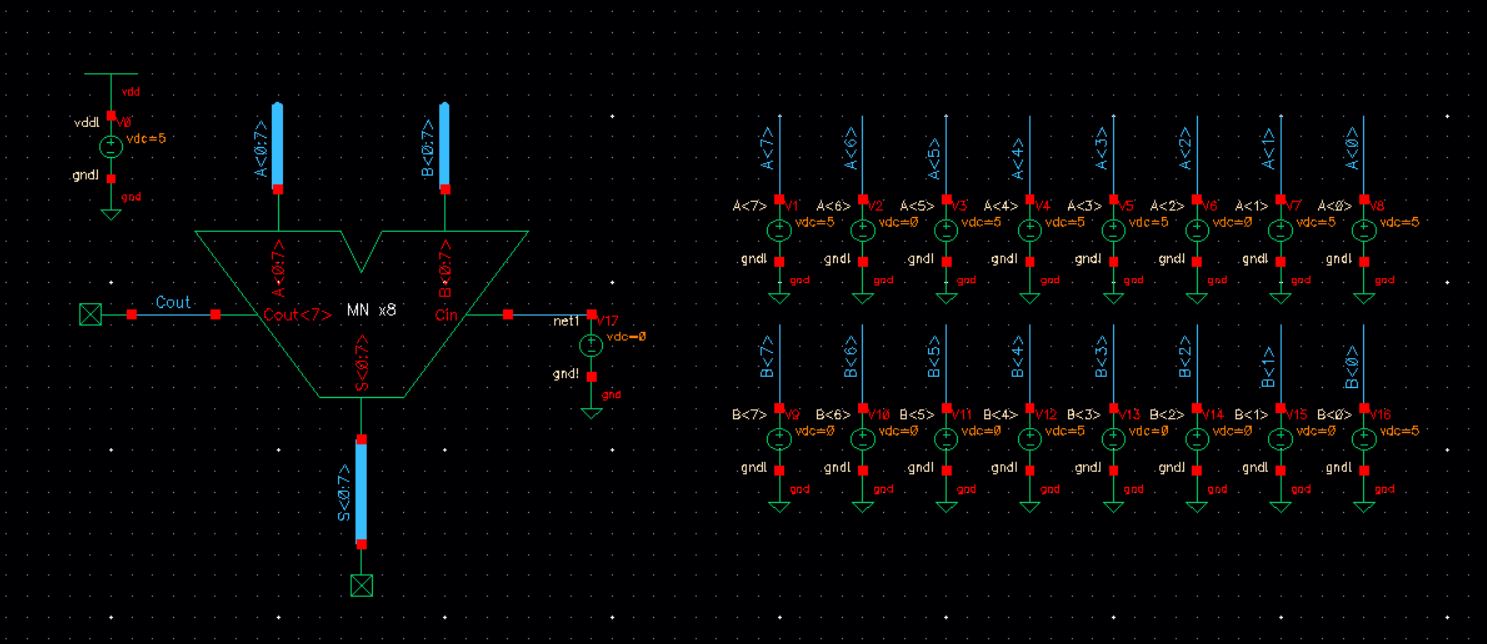
8-Bit AOI Full Adder
Schematic
Symbol
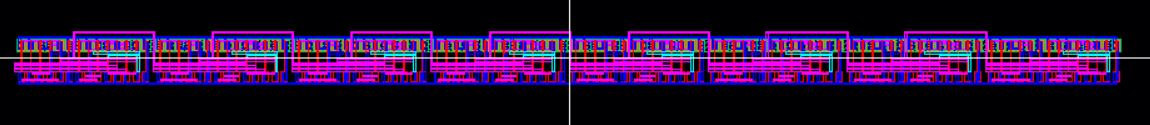
Layout

Extracted

DRC
LVS
Simulation
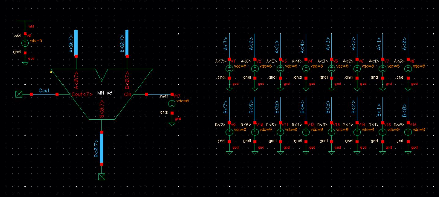
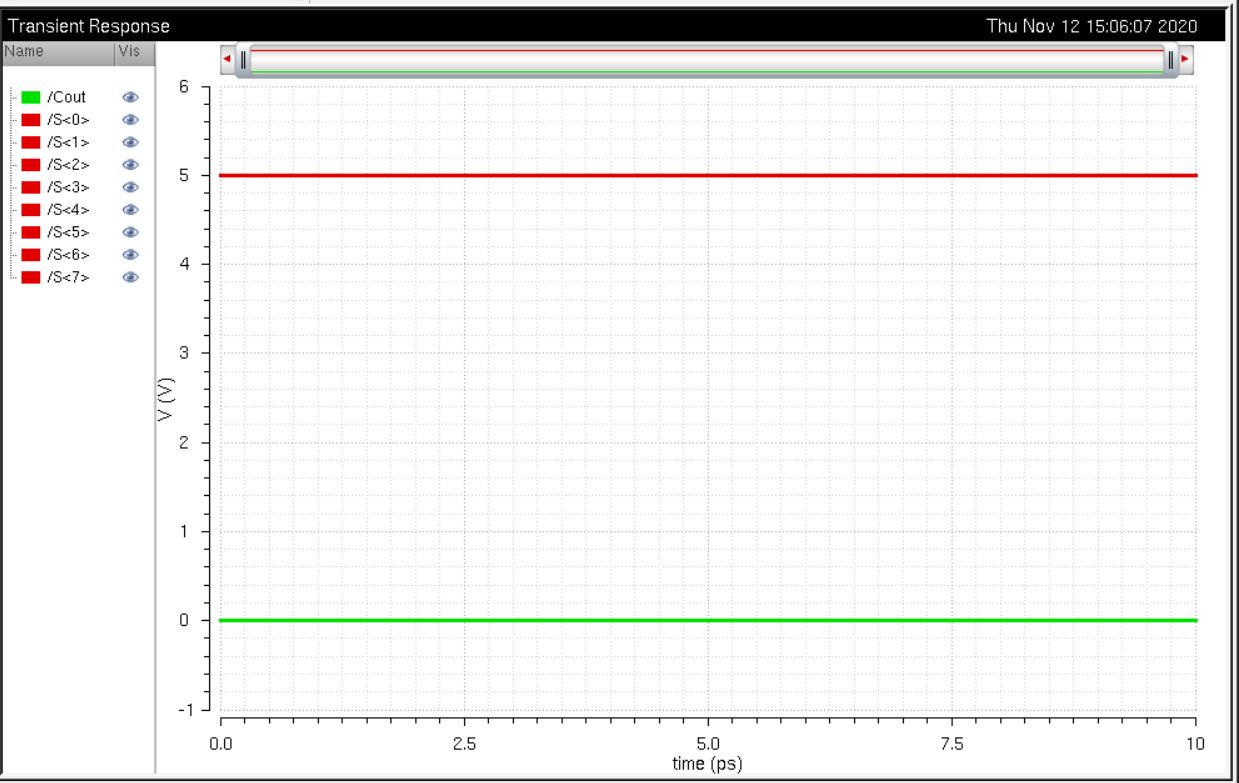
11111111 + 00000000 = 0 11111111 (256+0=256)
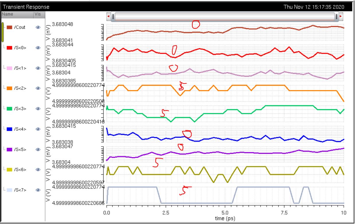
10111011 + 00010001 = 0 11001100 (187+17=204)