Lab 3 - EE 421L
Author: Michael Nguyen
Prelab:
Back-up all of your previous work from the lab and the course.
In the previous we made a DAC with a 2R and R voltage divider and simulated it.
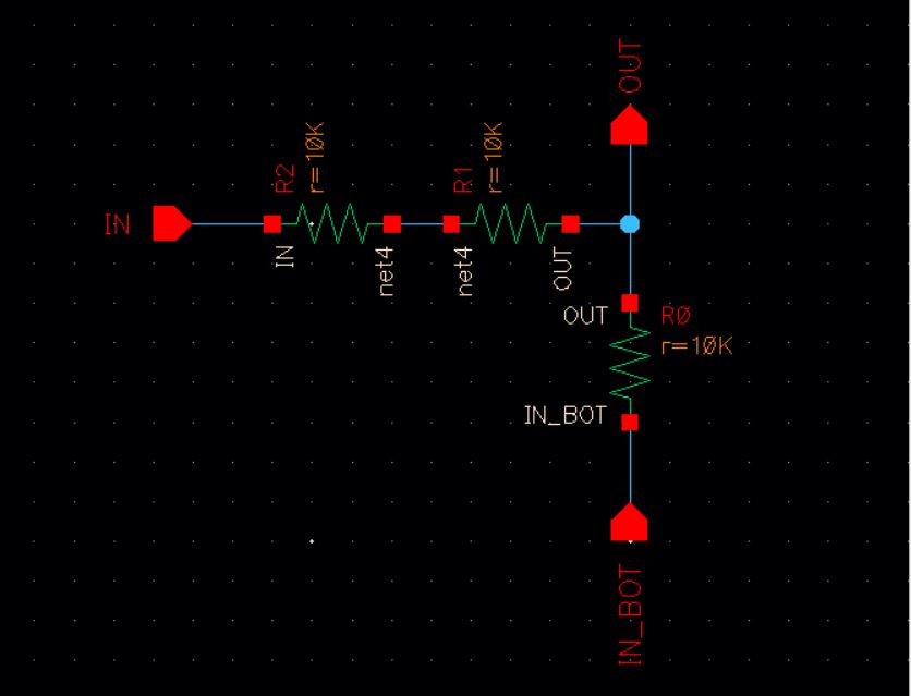
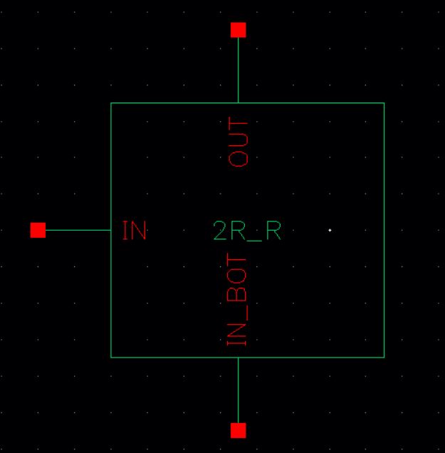
Figure 1
Figure 1 shows the 2R and R voltage divider schematic and symbol we made last last lab for our DAC
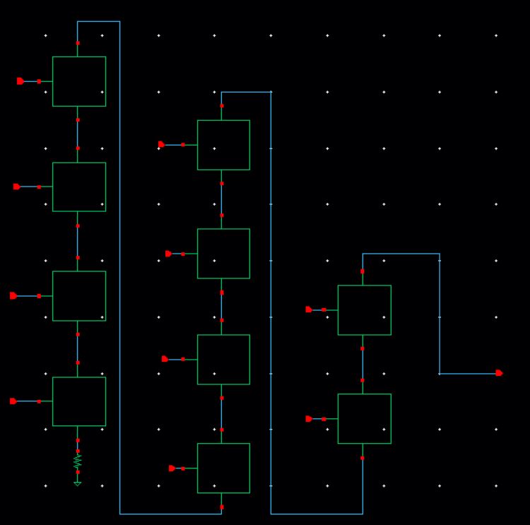
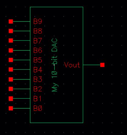
Figure 2
After creating the symbol of our voltage divider we used that to modify the ideal DAC given, to create the 10-bit DAC seen in Figure 2.
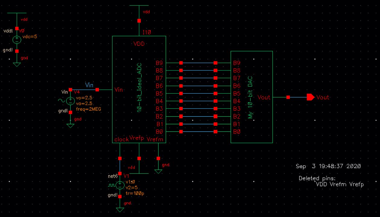
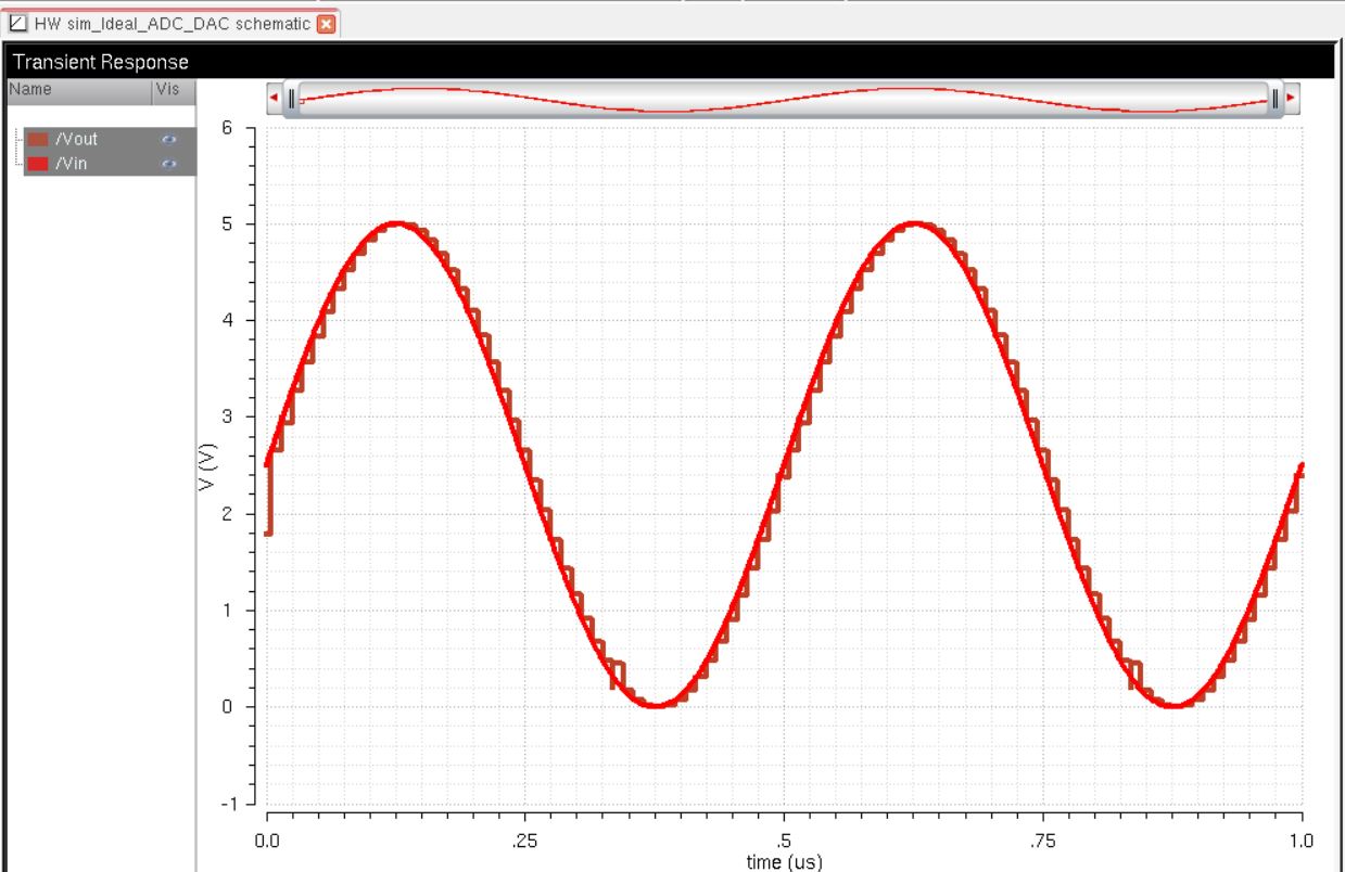
Figure 3
After creating our DAC we replace the ideal DAC with our created DAC in the schematic given in the last lab and simulated it, as seen in Figure 3.
Lab work:
In this lab we created they layout of the DAC we created and simulated last lab.
Starting out the lab by creating the 10K resistor N-well. For my N-well I used sheet resistance of 800Ω/sq and width of 3.6 microns.
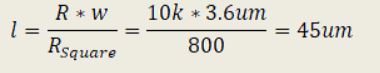
Above shows the calculations of the lenght equaling 45 microns.
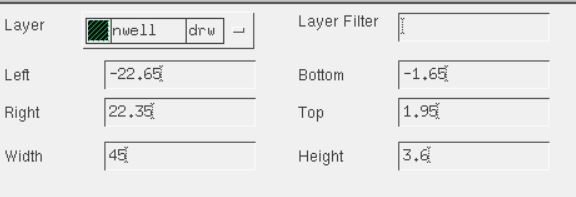
After the calculation, enter in the values to create the N-well, shown above are the lenght and width of the N-well.
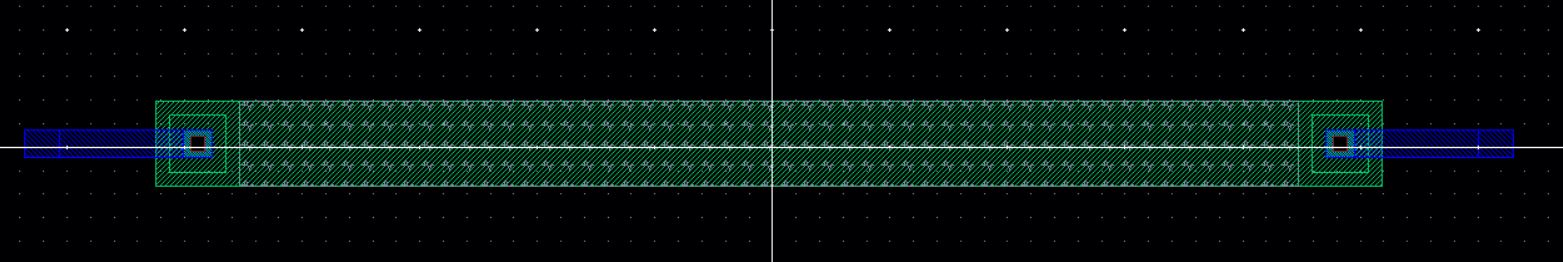
Following the steps on creating the N-well layed out in Tutorial 1 seen here, we get an N-well that is about 10.24KΩ.
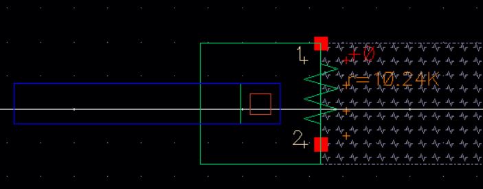
To make the process of creating the layout of the DAC a little easier, I decided to make the 2R and R voltage divider layout before doing the actual DAC.
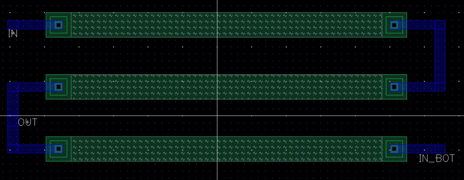
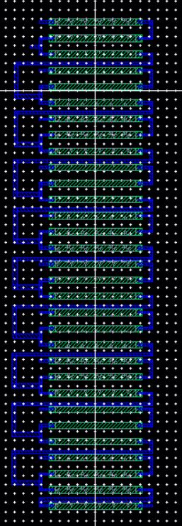
Using the voltage divider layout as seen above, we get the DAC layout seen below.
Completing all of that, it's time to check if it meets DRC guidlines and passes the LVS verification.
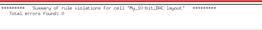
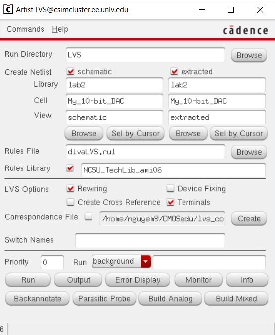
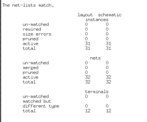
The layout passes both DRC and LVS.
Backing up the file by putting it into google drive.