Lab 7 - ECE 421L
| Schematic, Simulation Output and Layout of the ring oscillator |
||
|
|
|
|
||
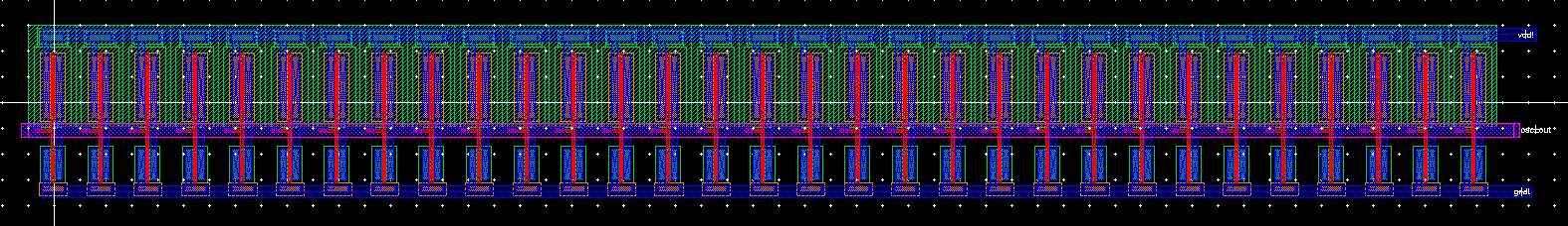
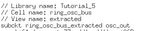
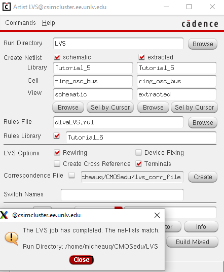
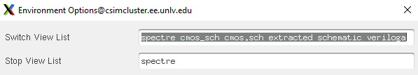
| LVS and proof that we are simulating the extracted version. |
||
 |
 |
 |
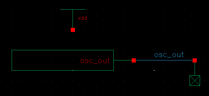
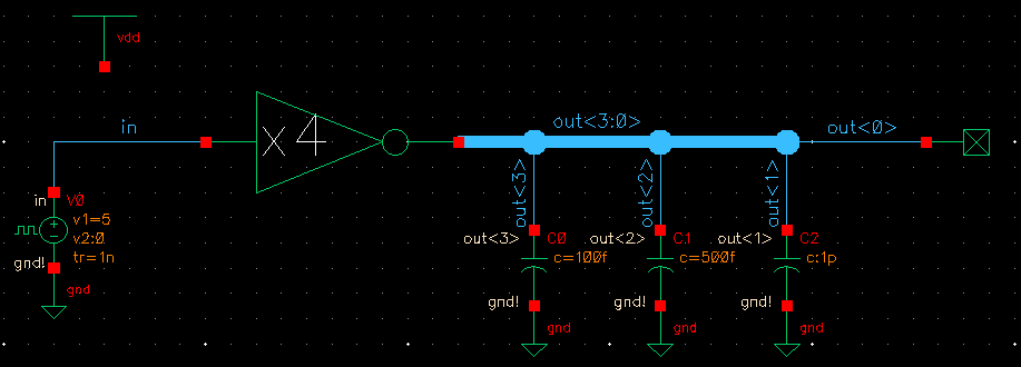
| Schematic |
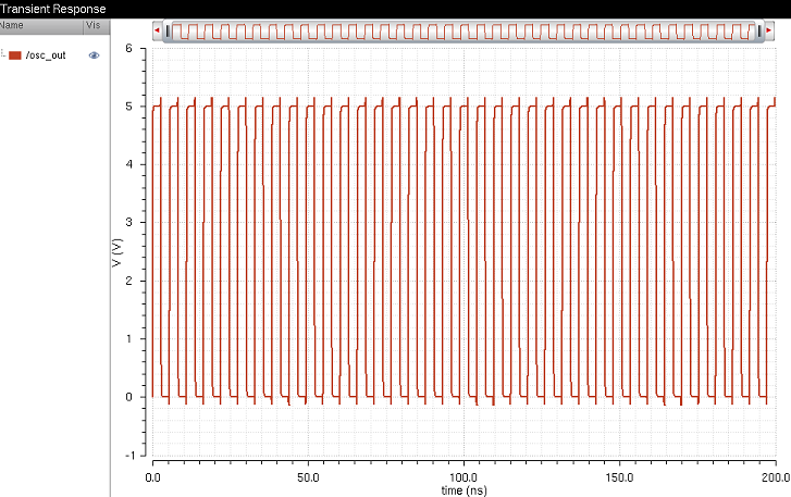
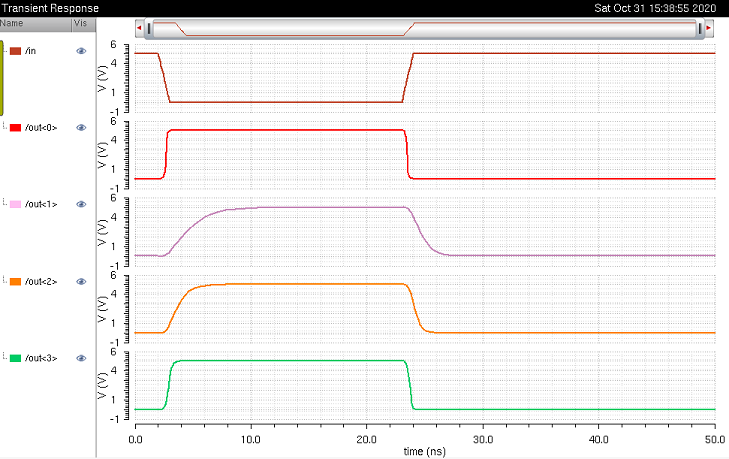
Simulation Results |
|
 |
 |
|
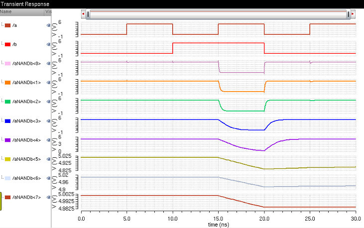
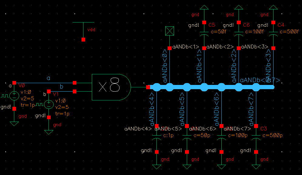
| 8-bit NAND Gate |
||
| Schematic |
Simulation Results |
|
|
 |
|
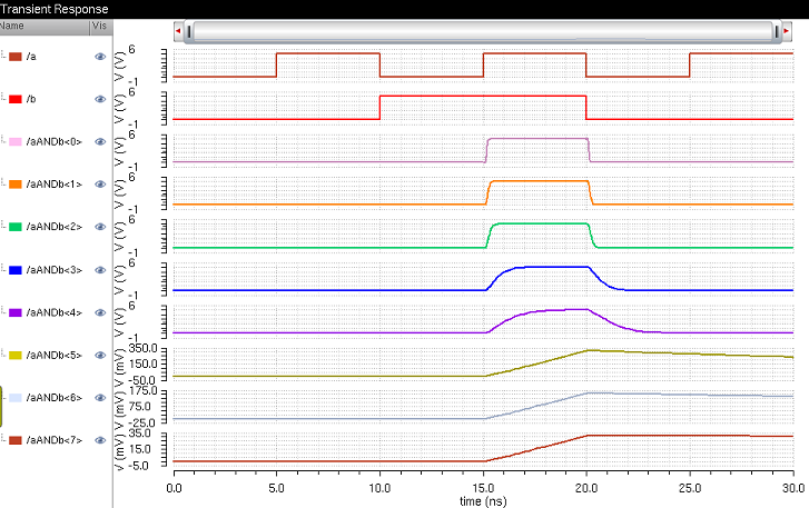
| 8-bit AND Gate |
|
| Schematic |
Simulation Results |
 |
 |
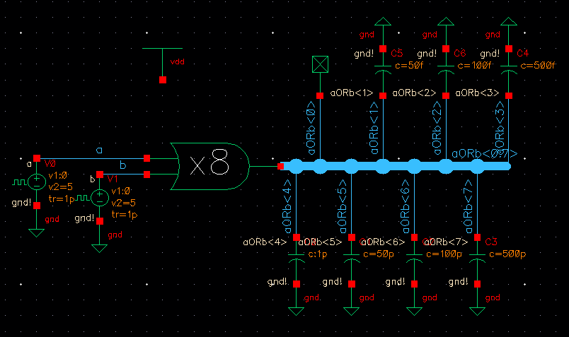
| 8-bit OR Gate |
|
| Schematic |
Simulation Results |
 |
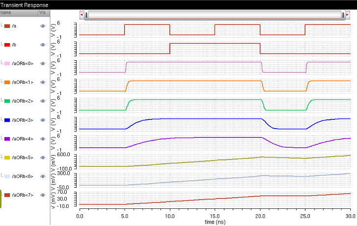 |
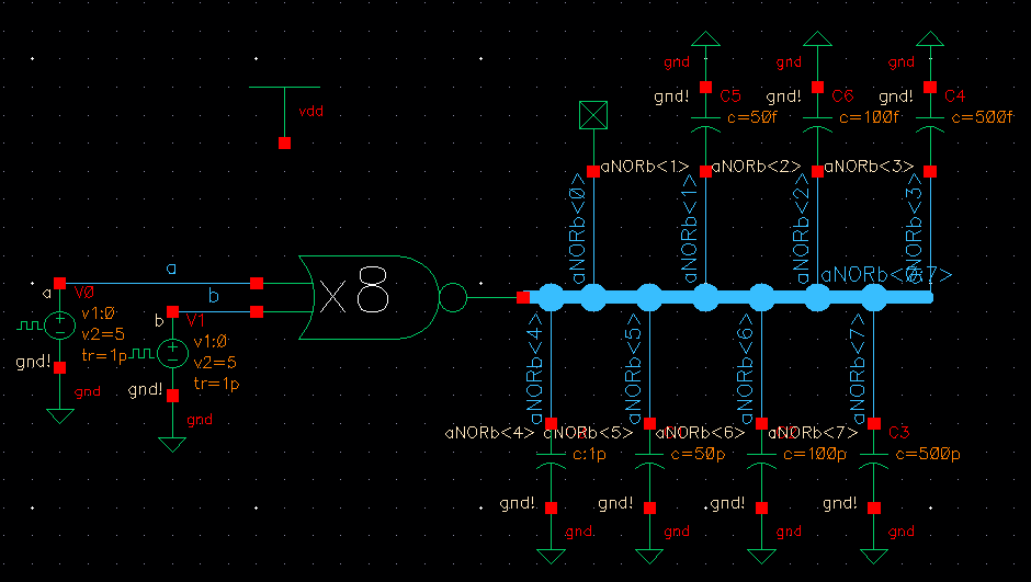
| 8-bit NOR Gate |
|
| Schematic |
Simulation Results |
 |
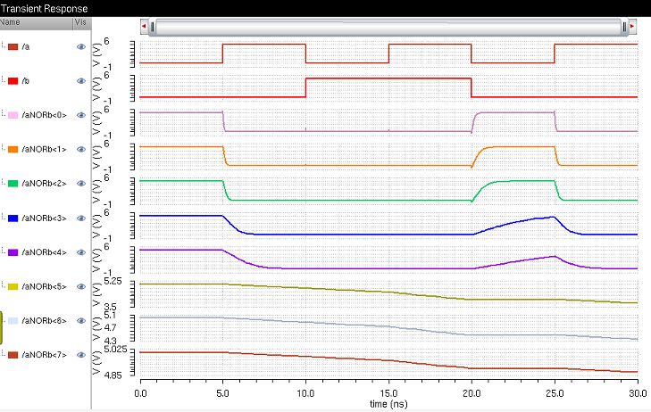 |
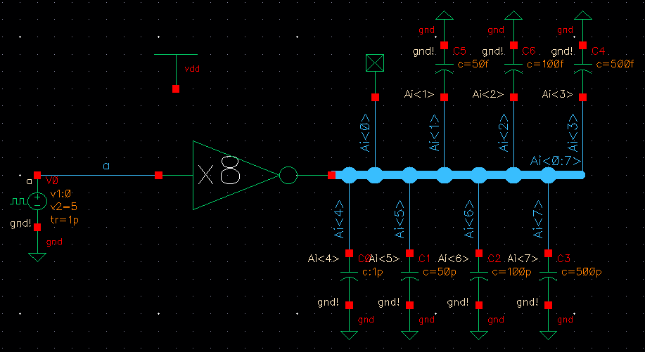
| 8-bit Inverter |
|
| Schematic |
Simulation Results |
 |
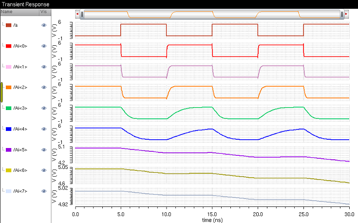 |
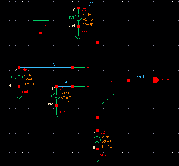
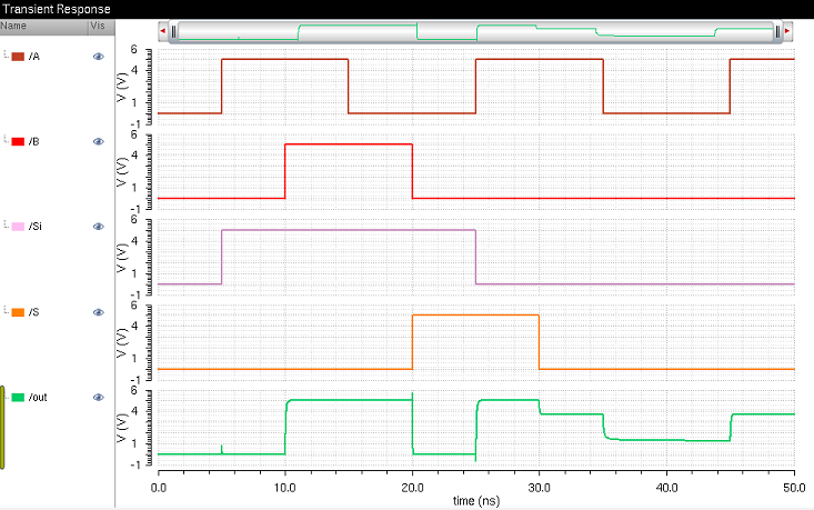
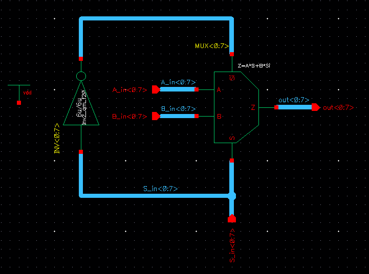
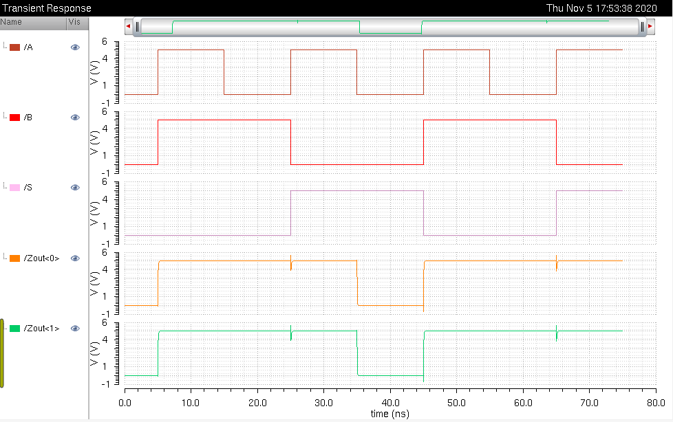
Below is the schematic and output of a MUX Gate
| Schematic |
Output Operation |
 |
 |
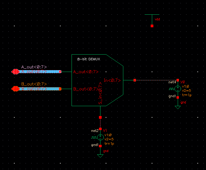
| Schematic |
Ouput |
 |
 |
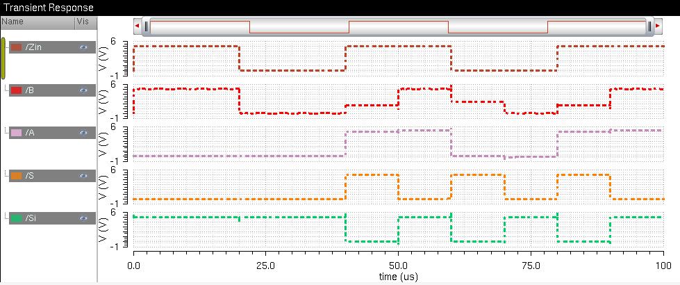
| Schematic |
Output |
 |
 |
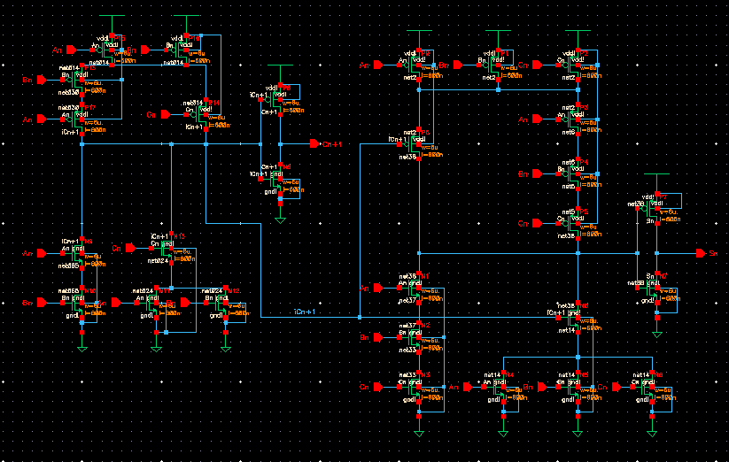
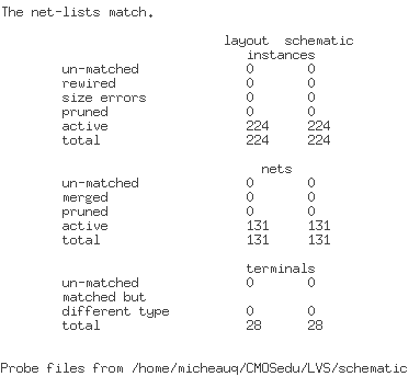
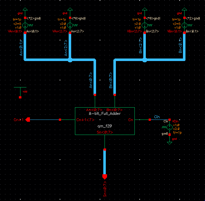
Below is the Schematic, Layout, Extracted Layout, LVS and Simulation of an 8 bit Full Adder.
| Single Bit Adder |
||
| Schematic |
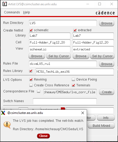
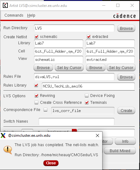
LVS |
|
 |
 |
|
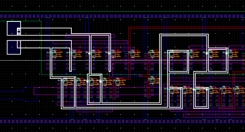
| Layout |
||
 |
||
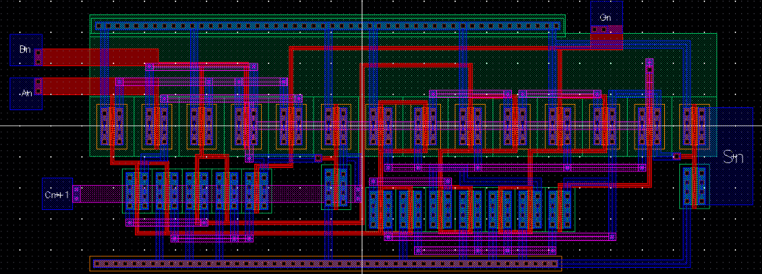
| Layout |
 |
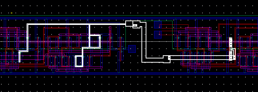
| Close up of Layout Section (Note: Total length of the layout is 1050 um or just barely 1mm) |
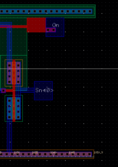 |
| Close up of Layout Section |
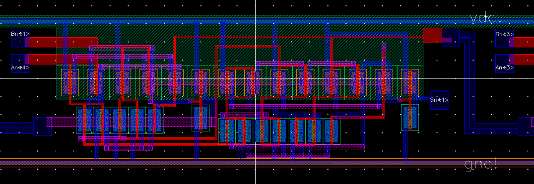 |
| Height Dimension of Layout (20 um Smaller than "thinner" than last design) |
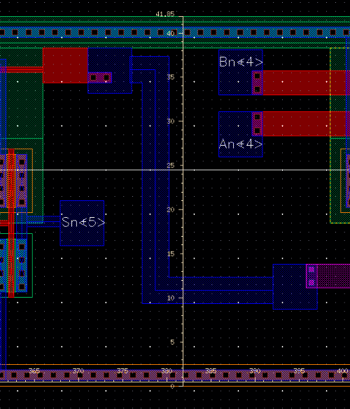 |
| Extracted view of Inputs An and Bn highlighted |
 |
| Extraced view of the carry-over bit |
 |
| LVS |
  |
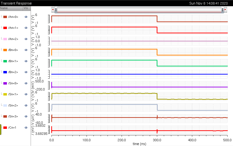
Bit Addition
The following operation will be performed by the circuit:
| Carry |
1 |
1 |
||||||
| An |
0 |
0 |
0 |
0 |
0 |
0 |
1 |
1 |
| Bn + |
0 |
0 |
0 |
0 |
0 |
0 |
1 |
1 |
| Sum |
0 |
0 |
0 |
0 |
0 |
1 |
1 |
0 |
And this is what we get in the simulation!
| Schematic |
Output |
 |
 |