Lab 6 - ECE 421L
Design, layout, and simulation of a CMOS NAND gate, XOR gate, and Full-Adder
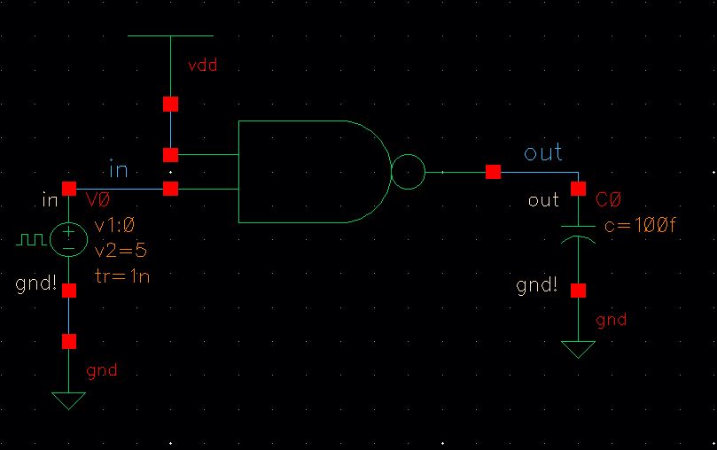
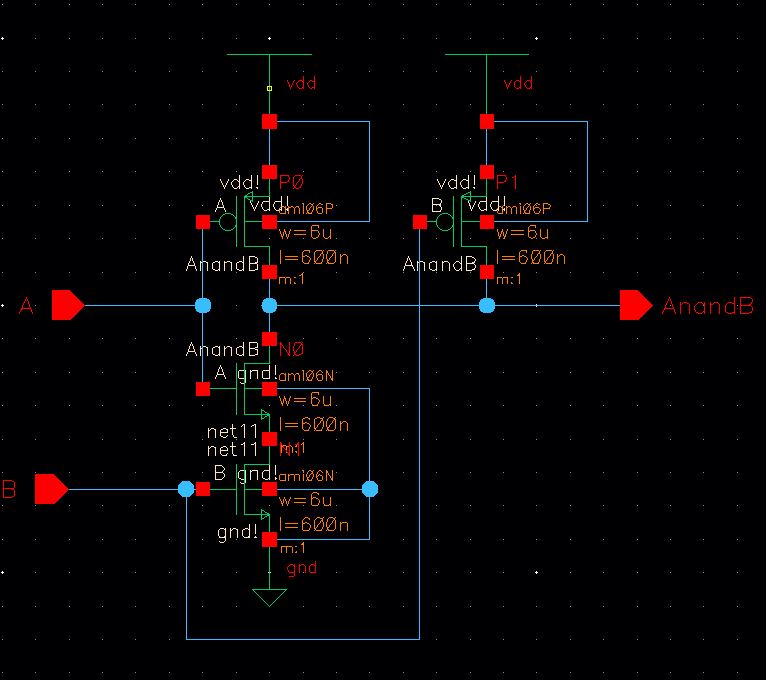
To start, Tutorial 4 goes over the basics of laying out and drawing the schematic of a NAND gate.
| Schmatic | Layout |
|
|
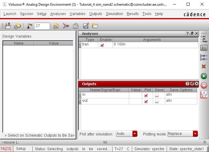
| Setup |
Results |
|
|
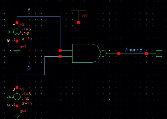
| Schematic |
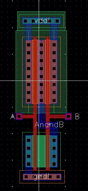
Layout |
 |
|
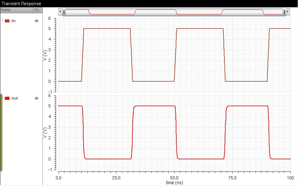
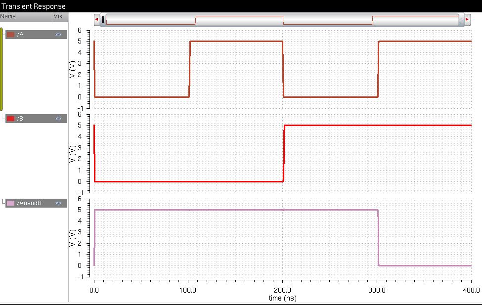
| Simulation |
|
 |
|
 |
|
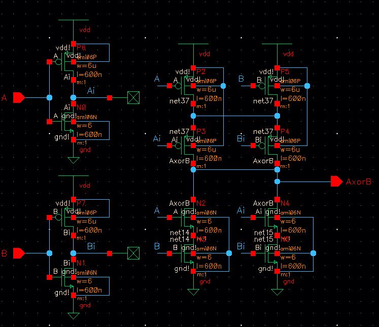
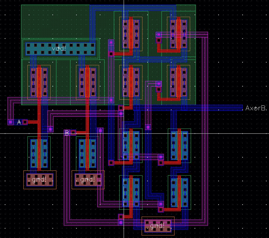
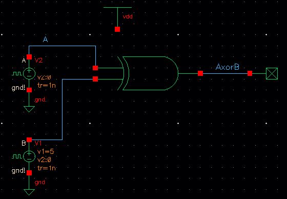
| Schematic |
Layout |
 |
 |
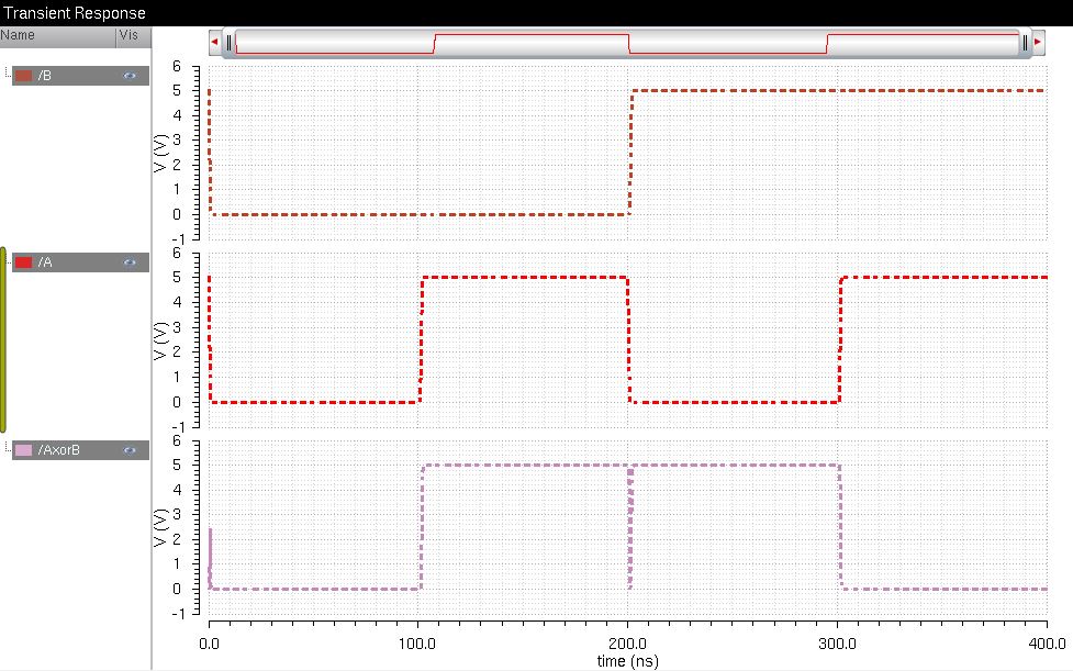
| Simulation |
|
 |
|
 |
|
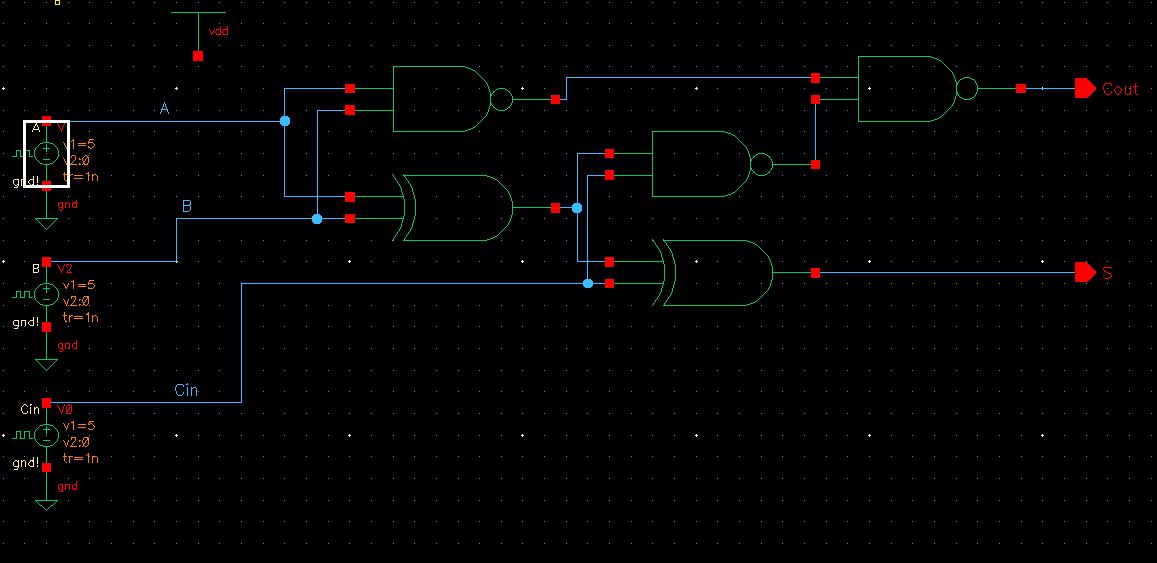
| Schematic |
|
 |
|
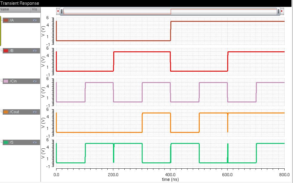
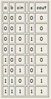
| Simulation results with Truth Table |
|
 |
 |
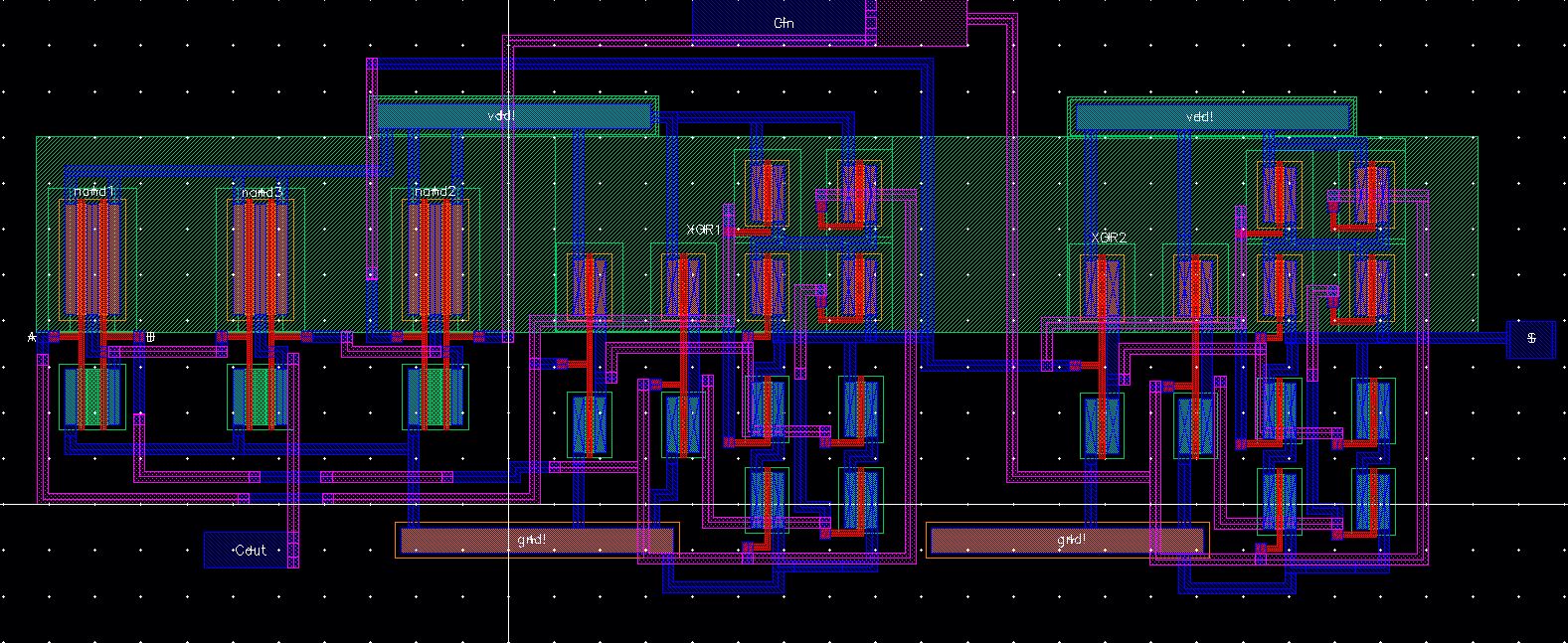
| Layout |
|
 |
|
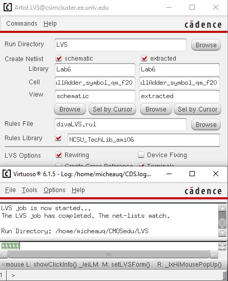
| LVS |
|
 |
|
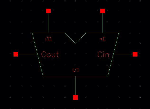
| Symbol |
 |
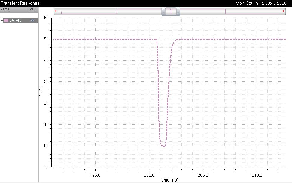
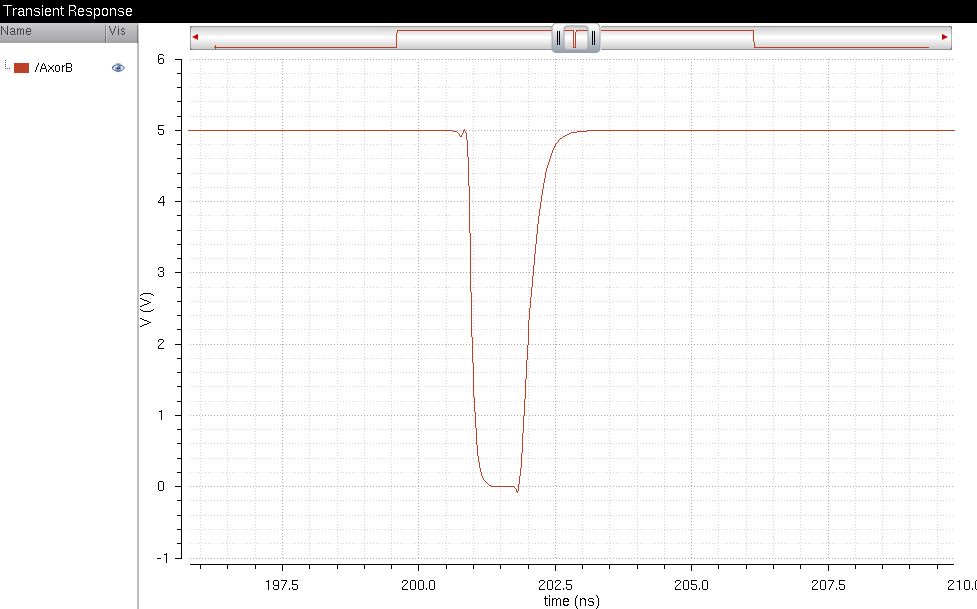
Glitches
|
| Zooming in on the glitch |
 |
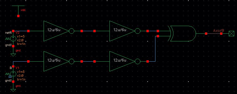
| 12u Inverter Buffer |
 |
 |
| 48u Inverter Buffer |
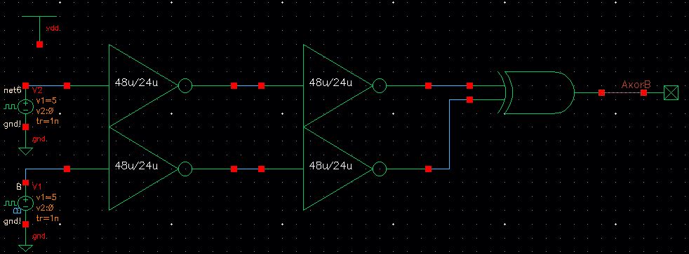 |
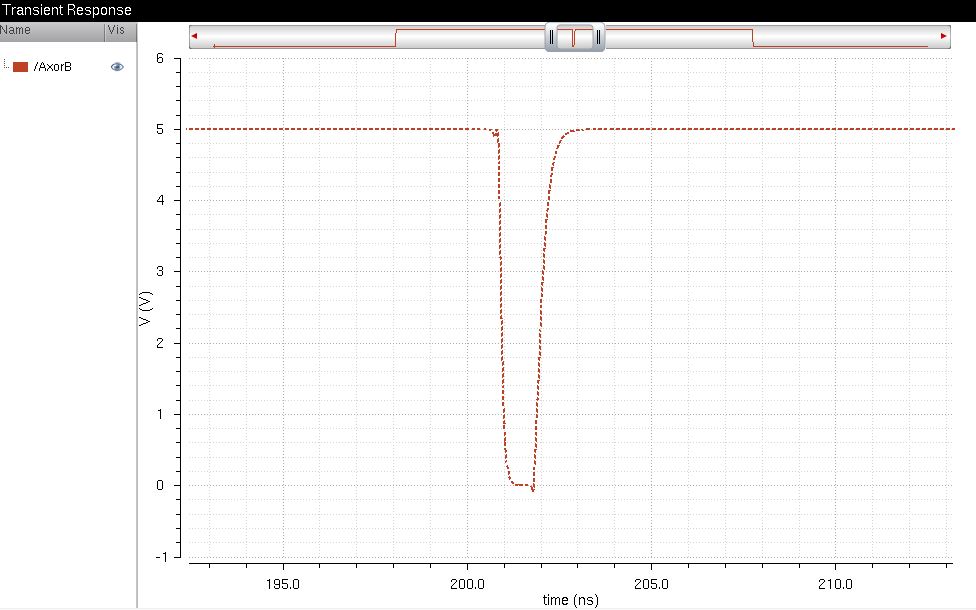 |
As see above, the glitching does apper to fade with the input coming from another logic gate.
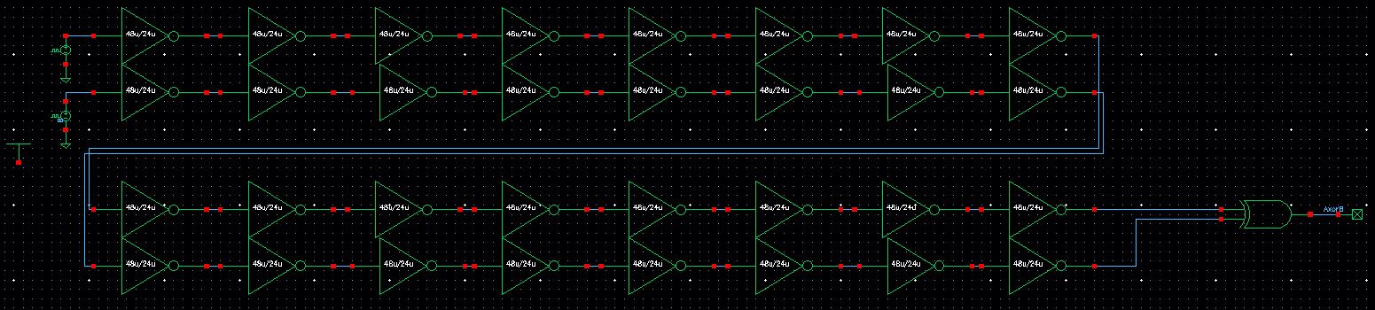
Now, taking the idea a bit further...
 |
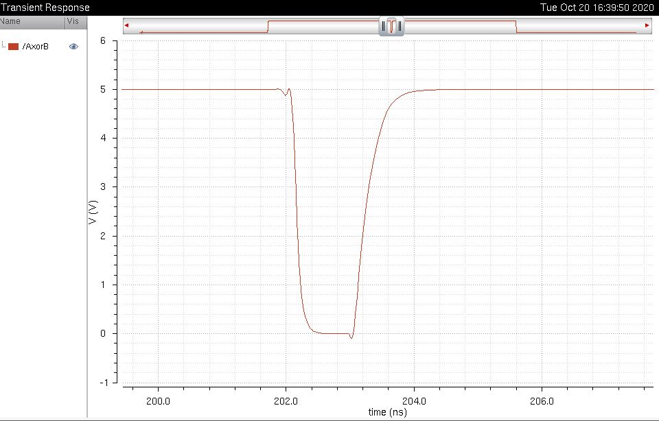 |
Unfortunately,
it appears as though since the gates cant change instantaneously, there
will always be a moment between switching where the output of the XOR2
gate will drop to zero. Even if it is less than a nanosecond.