Lab 4 - ECE 421L
Quinton Micheau
Today's
date
micheauq@unlv.nevada.edu
Lab 4
Lab
description:
In
this lab, we will be disigning and simulating NMOS and PMOS devices.
These two types of transistors can be found in almost any digital
device.
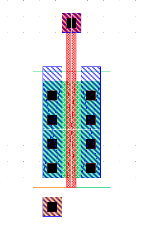
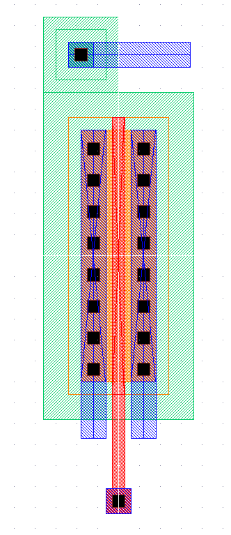
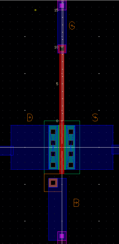
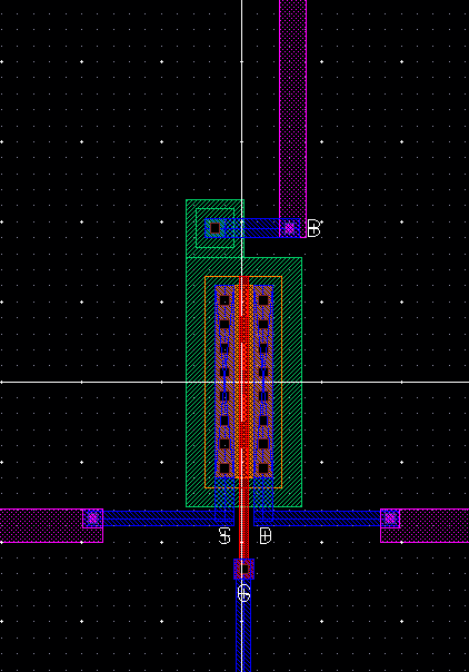
To start, the layout of the NMOS and PMOS transistors is presented:
NMOS
|
PMOS
|

|

|
Designs and Simulations:
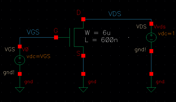
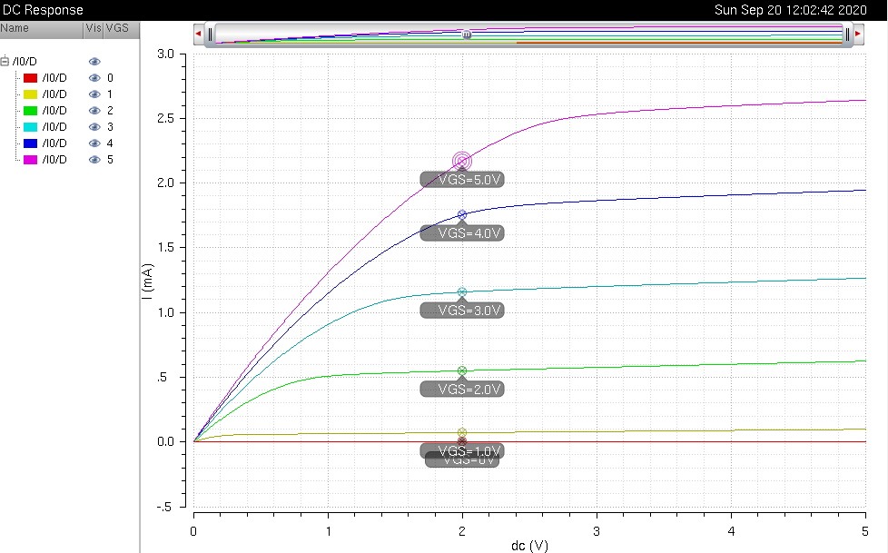
- A schematic for simulating ID
v. VDS of an NMOS device for VGS varying from 0 to 5 V in 1 V steps
while VDS varies from 0 to 5 V in 1 mV steps. Use a 6u/600n
width-to-length ratio.
- A
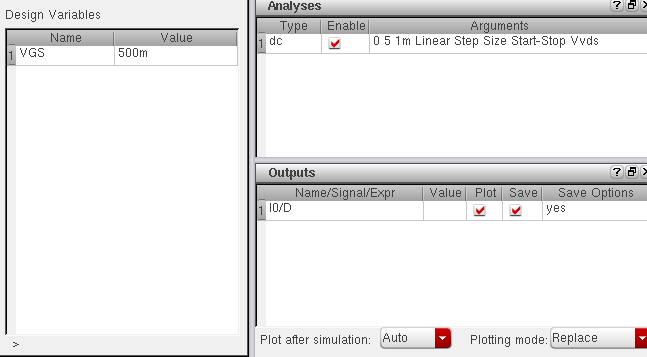
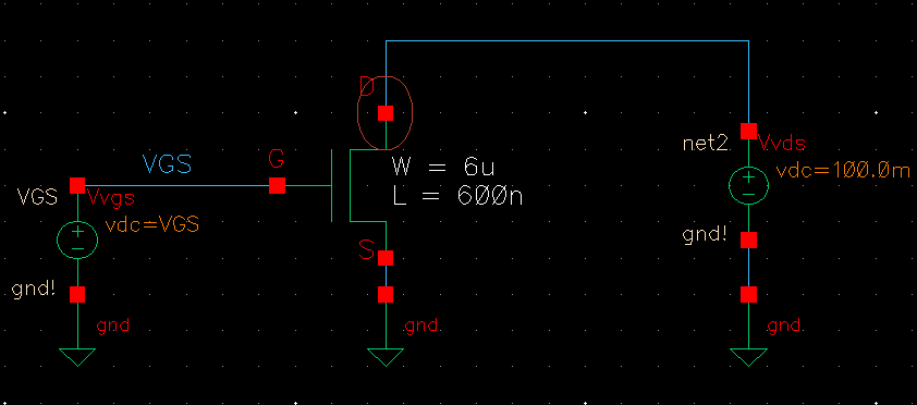
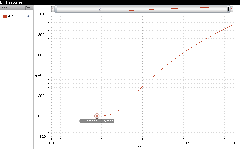
schematic for simulating ID v. VGS of an NMOS device for VDS = 100 mV
where VGS varies from 0 to 2 V in 1 mV steps. Again use a 6u/600n
width-to-length ratio.
- A
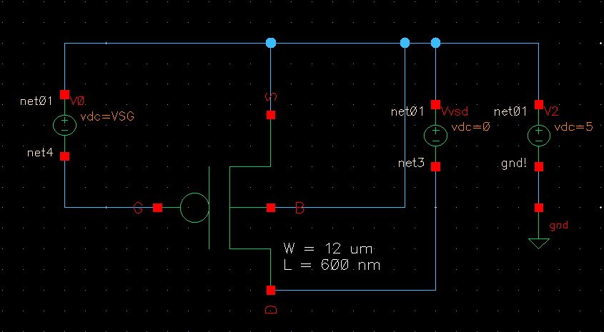
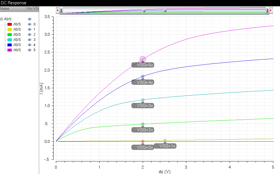
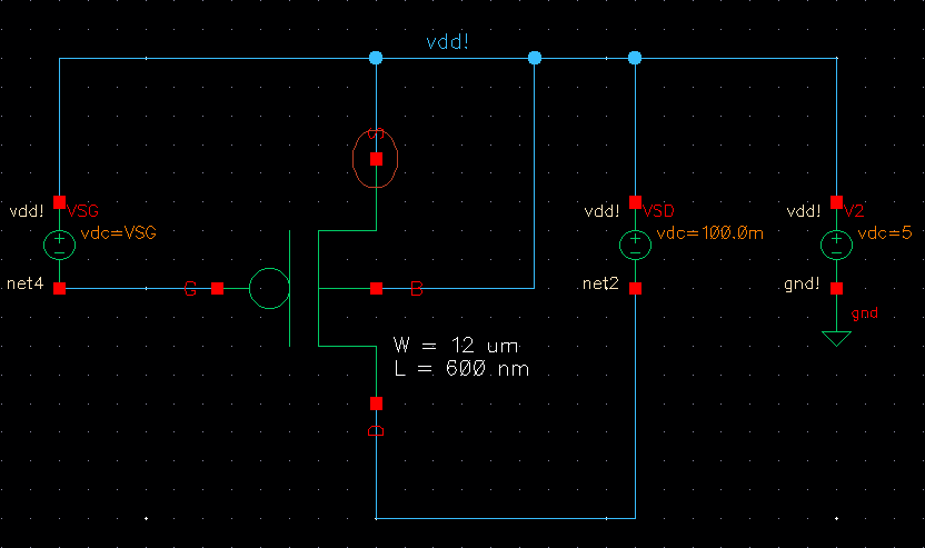
schematic for simulating ID v. VSD (note VSD not VDS) of a PMOS device
for VSG (not VGS) varying from 0 to 5 V in 1 V steps while VSD varies
from 0 to 5 V in 1 mV steps. Use a 12u/600n width-to-length ratio.
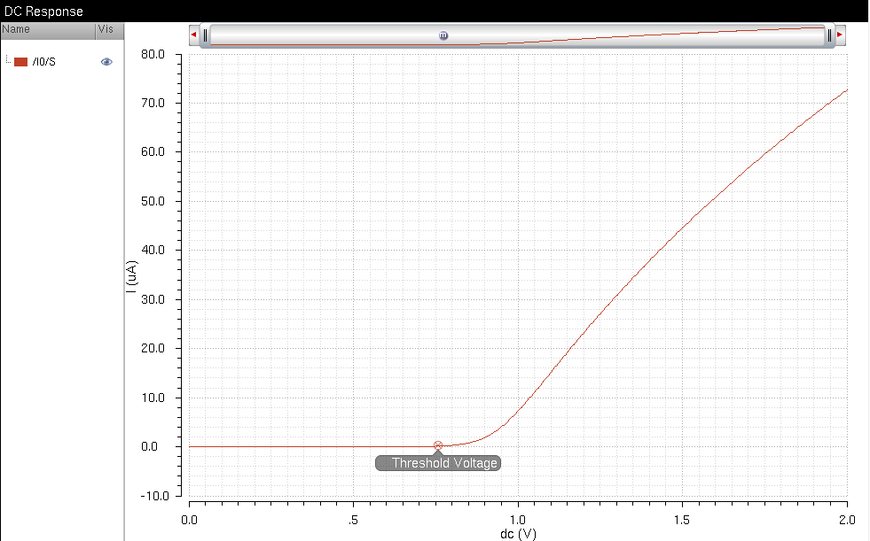
- A schematic for
simulating ID v. VSG of a PMOS device for VSD = 100 mV where VSG varies
from 0 to 2 V in 1 mV steps. Again, use a 12u/600n width-to-length
ratio.
Probe Pads
Schematics and symbols for Probe Pads are found in lab4.zip.
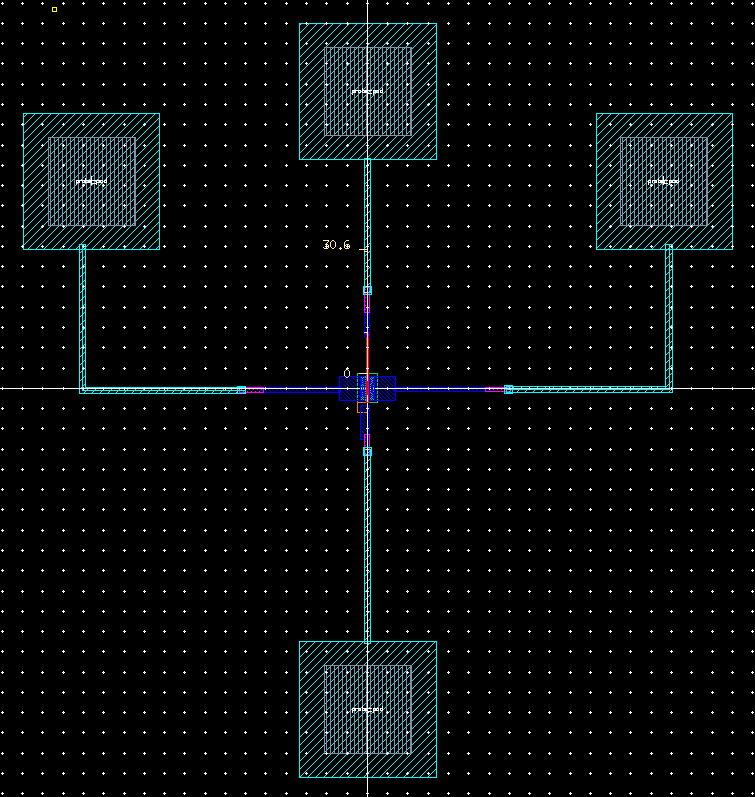
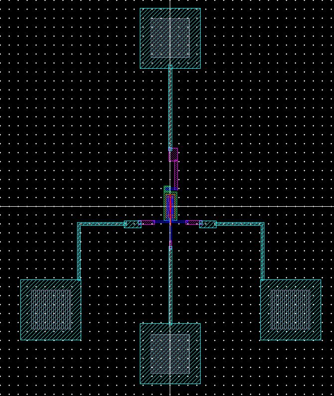
- Lay
out a 6u/0.6u NMOS device and connect all 4 MOSFET terminals to probe
pads (which can be considerably smaller than bond pads [see MOSIS design rules] and directly adjacent to the MOSFET (so the layout is relative small).
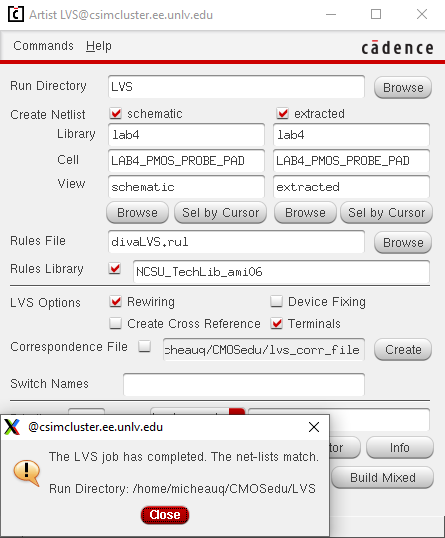
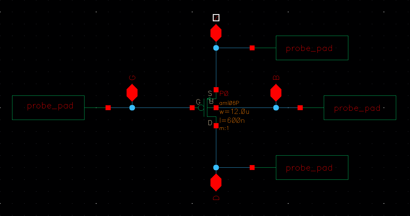
- Lay out a 12u/0.6u PMOS device and connect all 4 MOSFET terminals to probe pads.
Return to EE 421L Labs
