Lab 3 - ECE 421L
Quinton Micheau
9/3/2020
micheauq@unlv.nevada.edu
Lab 3
This week's laboratory will cover how to complete the layout view of
the 10-bit DAC we designed in the previous week.
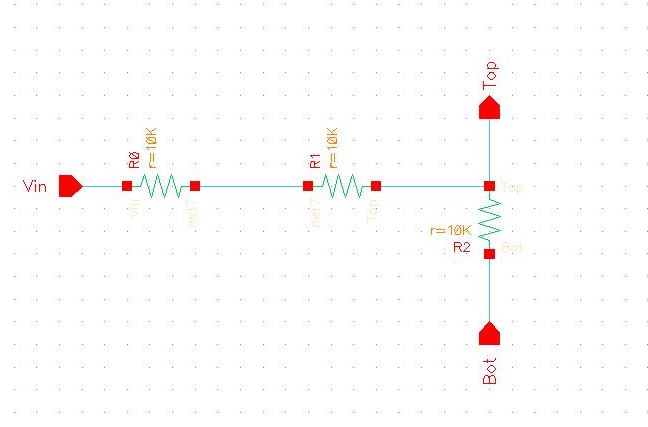
The DAC functions as a voltage devider so we need to construct a n-well equivalent layout of the 2R_R schematic shown below:
![http://cmosedu.com/jbaker/courses/ee421L/f20/students/micheauq/Lab%202/Images/Lab%202%20-5.JPG](http://cmosedu.com/jbaker/courses/ee421L/f20/students/micheauq/Lab%202/Images/Lab%202%20-5.JPG)
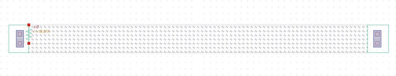
Following Tutorial_1, I designed an 10.01k n-well resistor shown below:
![http://cmosedu.com/jbaker/courses/ee421L/f20/students/micheauq/Lab%203/Images/Lab3-2.JPG](http://cmosedu.com/jbaker/courses/ee421L/f20/students/micheauq/Lab%203/Images/Lab3-2.JPG)
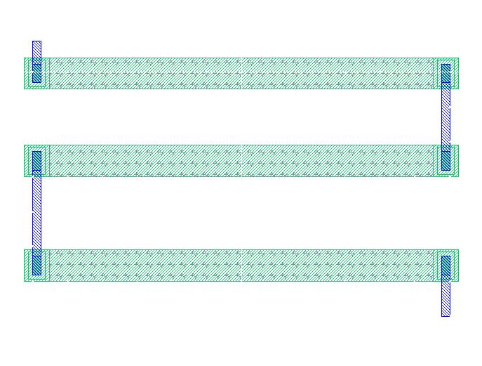
I combined these n-well resistors in an orientation that will give the same results as the 2R_R resistor:
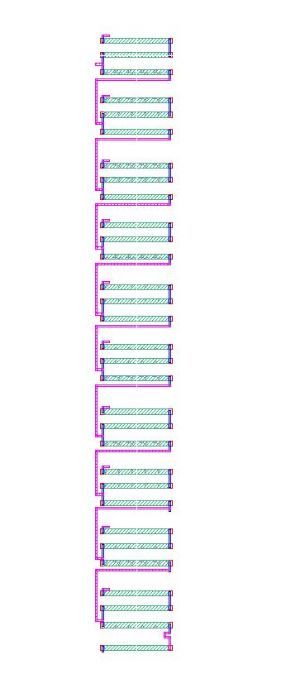
![http://cmosedu.com/jbaker/courses/ee421L/f20/students/micheauq/Lab%203/Images/Lab3-3.jpg](http://cmosedu.com/jbaker/courses/ee421L/f20/students/micheauq/Lab%203/Images/Lab3-3.jpg)
The
schematic we are drawing the layout for has 10 pins and each of the
above modules are a component for a single pin. Therefore, we need to
combine 10 of the above layout in order to complete our layout of the
10-bit DAC. Below is the layout for the 10-bit DAC using n-well
resistors and connecting them with metal_2.
![http://cmosedu.com/jbaker/courses/ee421L/f20/students/micheauq/Lab%203/Images/Lab3-4.JPG](http://cmosedu.com/jbaker/courses/ee421L/f20/students/micheauq/Lab%203/Images/Lab3-4.JPG)
Changing the layer view shows that our 10-bit DAC is built from individual 2R_R's we designed previously.
![http://cmosedu.com/jbaker/courses/ee421L/f20/students/micheauq/Lab%203/Images/Lab3-6.JPG](http://cmosedu.com/jbaker/courses/ee421L/f20/students/micheauq/Lab%203/Images/Lab3-6.JPG)
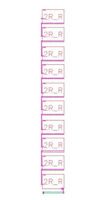
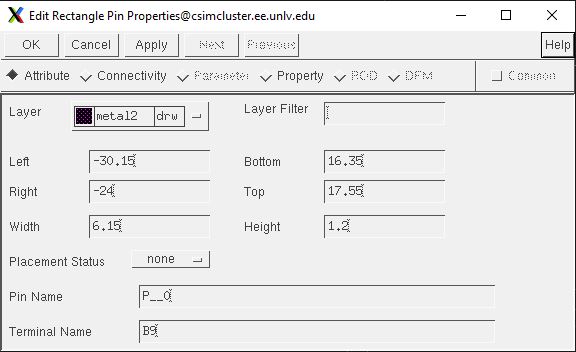
Each 2R_R block has a corresponding pin B0-B9:
![http://cmosedu.com/jbaker/courses/ee421L/f20/students/micheauq/Lab%203/Images/Lab3-7.JPG](http://cmosedu.com/jbaker/courses/ee421L/f20/students/micheauq/Lab%203/Images/Lab3-7.JPG)
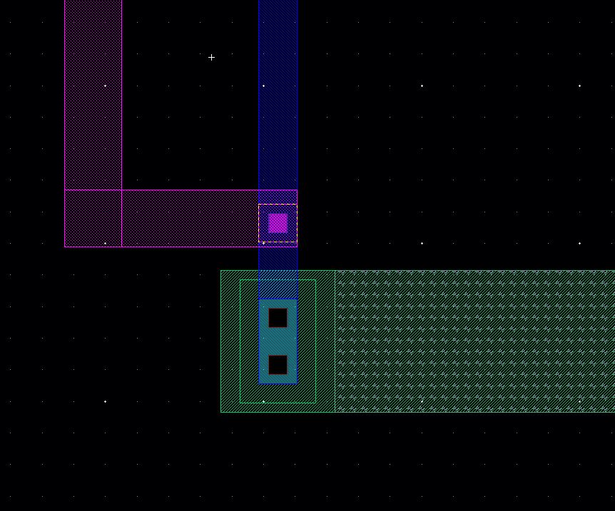
Metal_1 and metal_2 are connected via the instance M1_M2 found in the appropriate ami library.
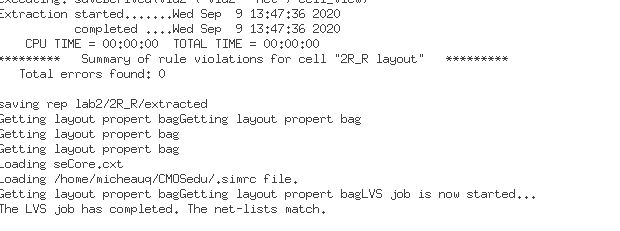
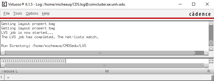
![http://cmosedu.com/jbaker/courses/ee421L/f20/students/micheauq/Lab%203/Images/Lab3-5.JPG](http://cmosedu.com/jbaker/courses/ee421L/f20/students/micheauq/Lab%203/Images/Lab3-5.JPG)
Finally,
in order to ensure that our layout and schematic are compliant with the
Cadence design rules, a DRC was run as well as an LVS verification.
Both results showed that the layout is indeed the same as the schematic
and that the design follows the rules.
![http://cmosedu.com/jbaker/courses/ee421L/f20/students/micheauq/Lab%203/Images/Lab3.JPG](http://cmosedu.com/jbaker/courses/ee421L/f20/students/micheauq/Lab%203/Images/Lab3.JPG)
![http://cmosedu.com/jbaker/courses/ee421L/f20/students/micheauq/Lab%203/Images/Lab3-1.JPG](http://cmosedu.com/jbaker/courses/ee421L/f20/students/micheauq/Lab%203/Images/Lab3-1.JPG)
Zip file for the above schematics
Return to EE 421L Labs