Lab 7 - EE 421L
Authored
by Peter Kim
kimj98@unlv.nevada.edu
11/4/2020
Prelab:
- Back-up all of your work from the lab and the course
(all work is backed-up on USB drive, and on google drive)
- Go through Tutorial 5
- Read through the entire lab
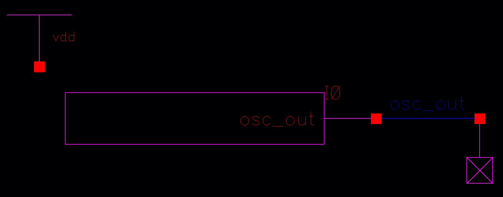
Schematic of Ring Oscillator:

Layout of Ring Oscillator:
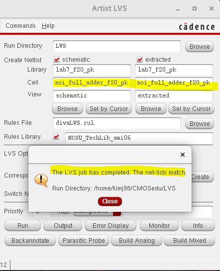
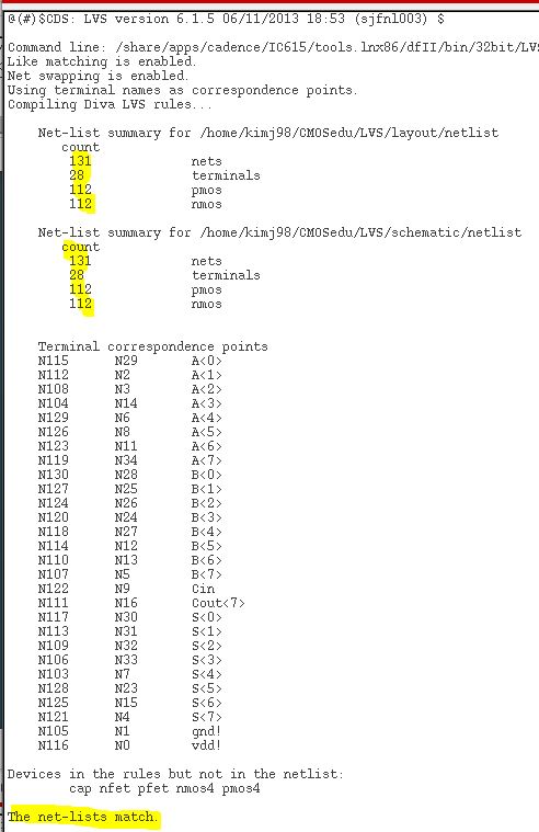
LVS result:


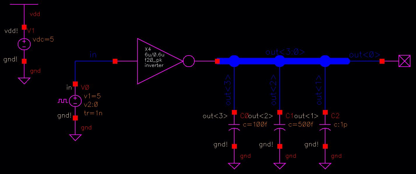
Simulation Schematic:
Simulation Plot (blue - schematic view, Red - extracted view, note: plots didn't match, extracted view is faster)

LAB Report:
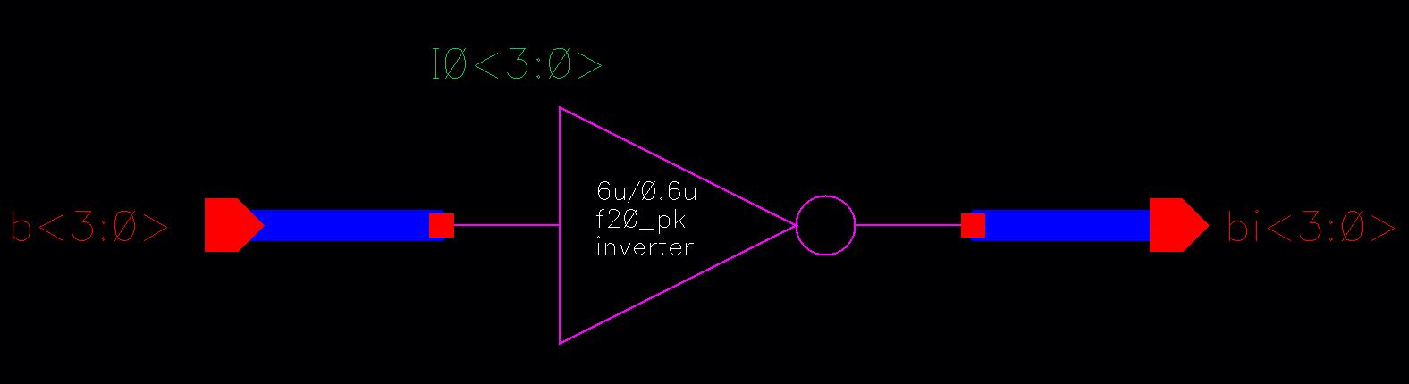
- Examine and simulate the circuit used for inverting a 4-bit word seen below:
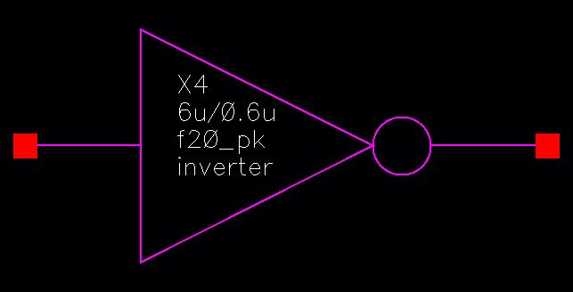
X4 inverter shown above is comprised of following cells:
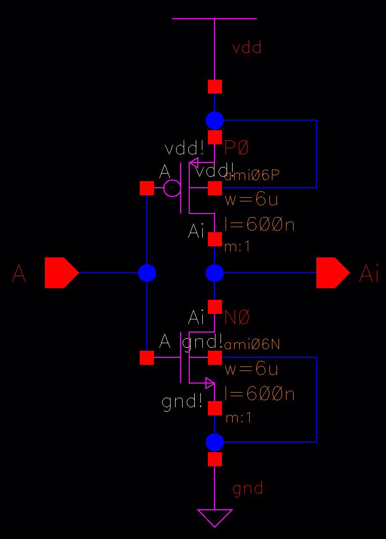
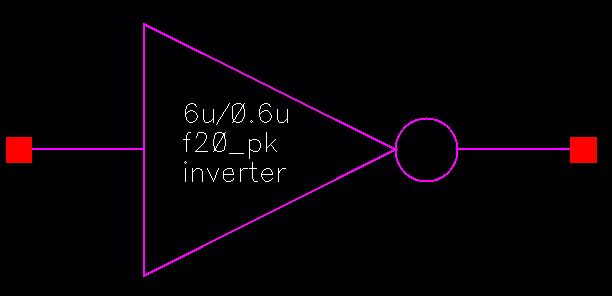
(schematic of inverter (6u/0.6 NMOS & PMOS), symbol of inverter, schematic of 4X inverter, symbol of 4X inverter):
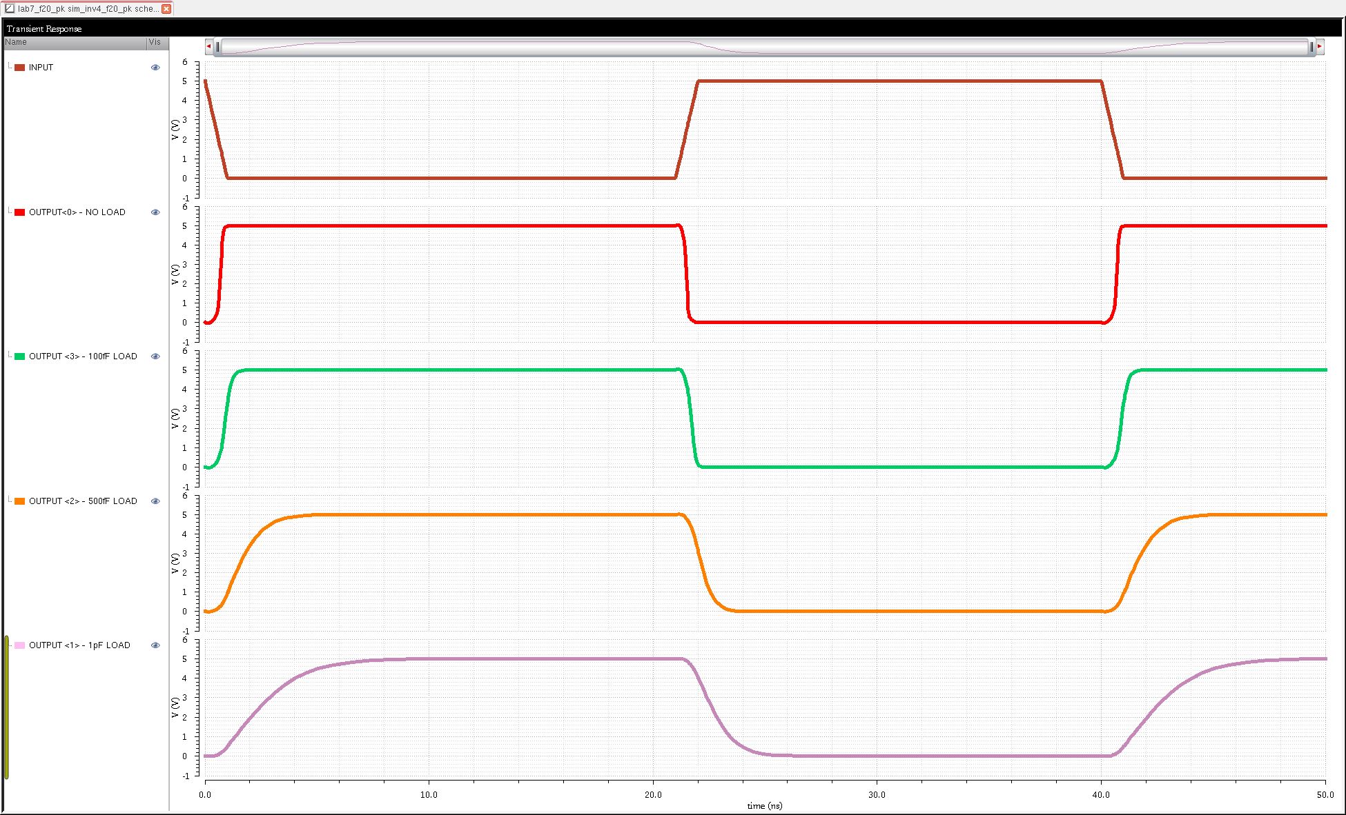
Simulation result:
- From the simulation plot, as the load capacitance
gets larger, the RC time delay of output gets longer.
-
Create schematics and symbols for and 8-bit input/output array of:
NAND, NOR, AND, INVERTER and OR gates (show simulation using these
gates).
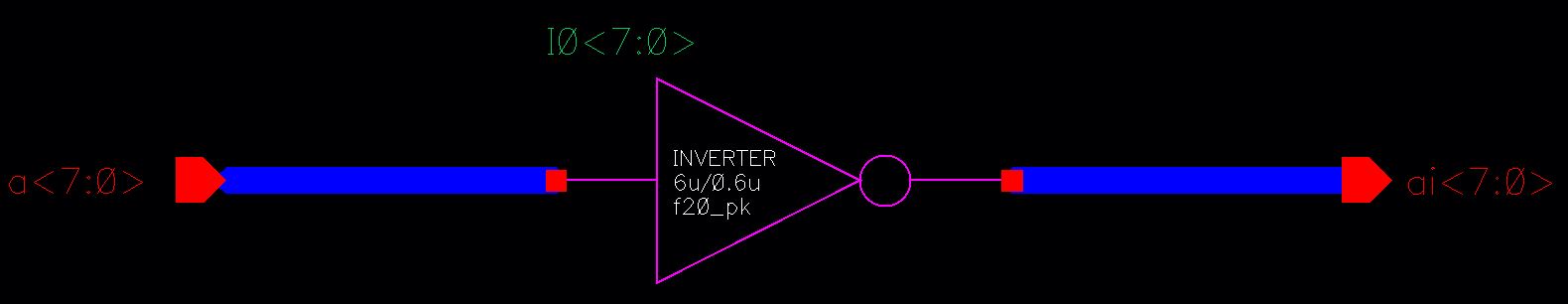
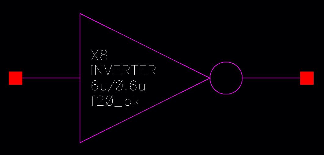
- Schematic & symbol of 8-bit INVERTER
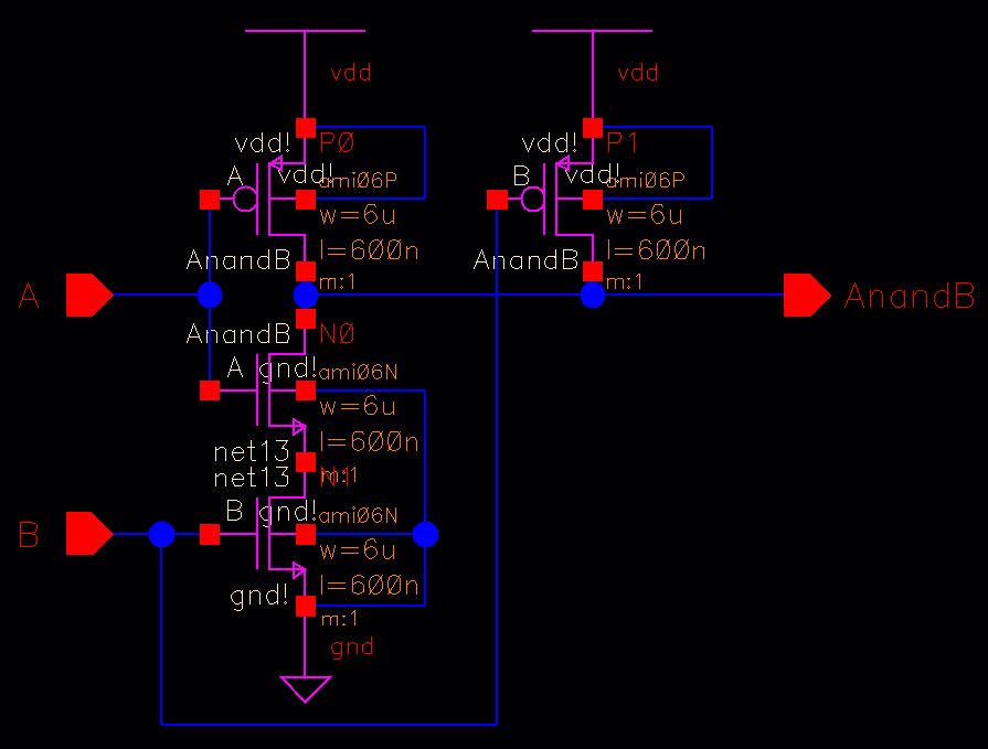
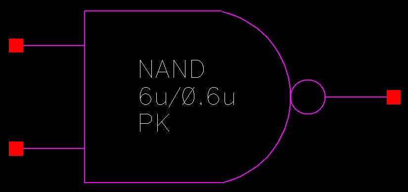
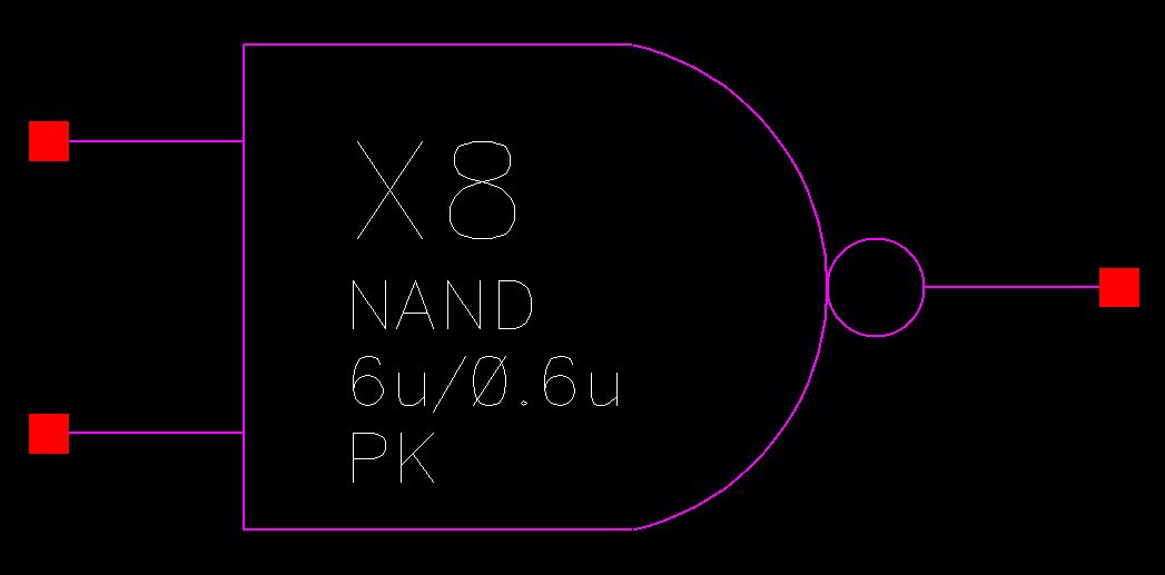
- Schematic & symbol of 2 input NAND gate & 8-bit NAND gate

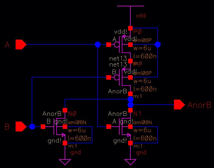
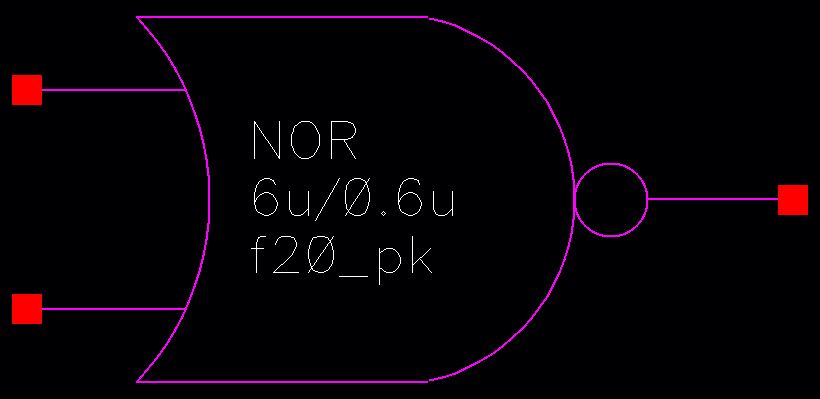
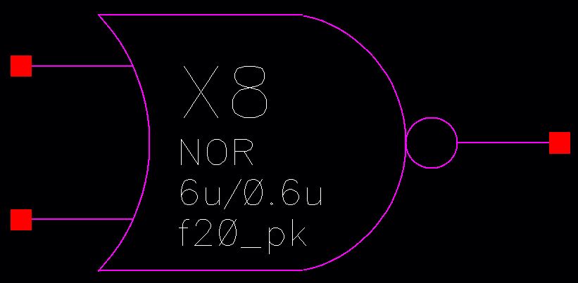
- Schematic & symbol of 2 input NOR gate & 8-bit NOR gate

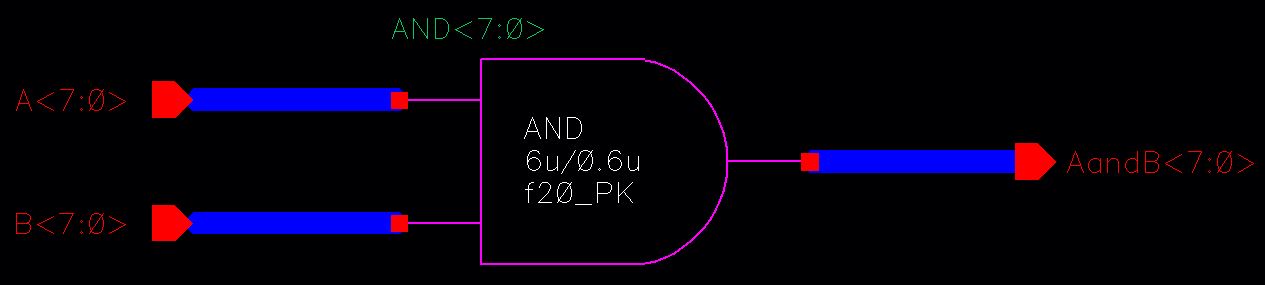
- Schematic & symbol of 2 input AND gate & 8-bit AND gate


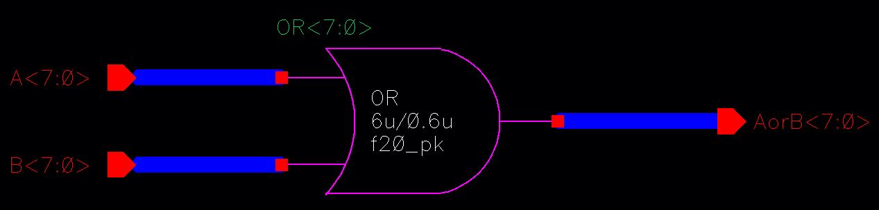
- Schematic & symbol of 2 input OR gate & 8-bit OR gate


- Run Simulations:
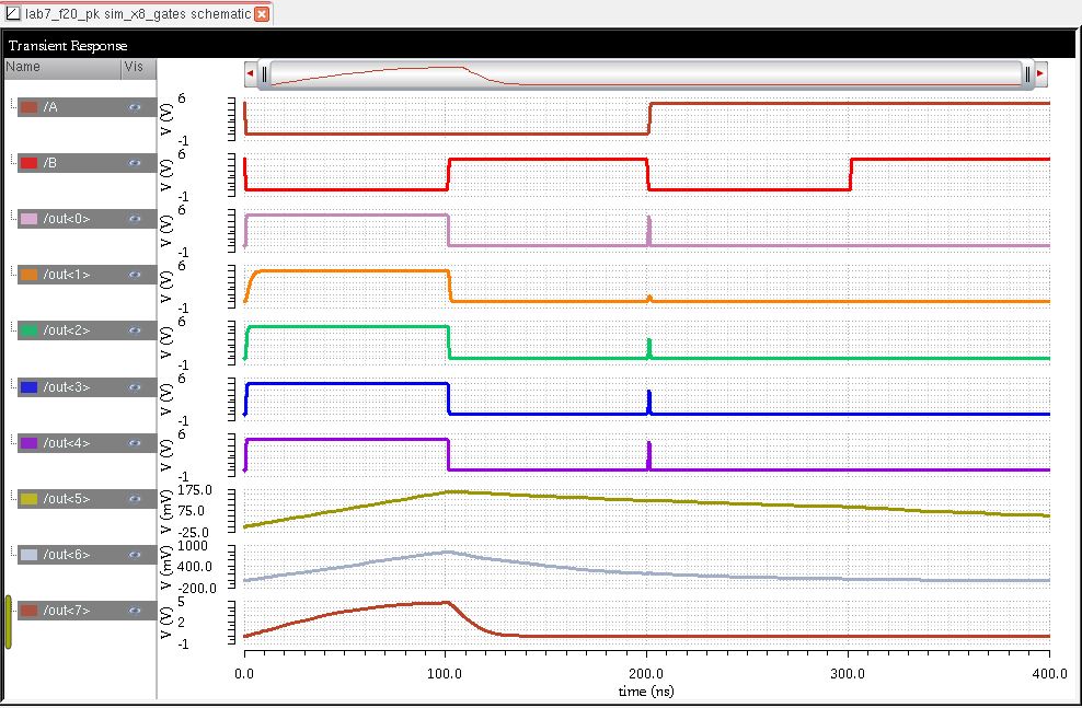
Schematic and simulation plot for 8-bit inverter

Schematic and simulation plot for 8-bit AND gate:

Schematic and simulation plot for 8-bit NAND gate:

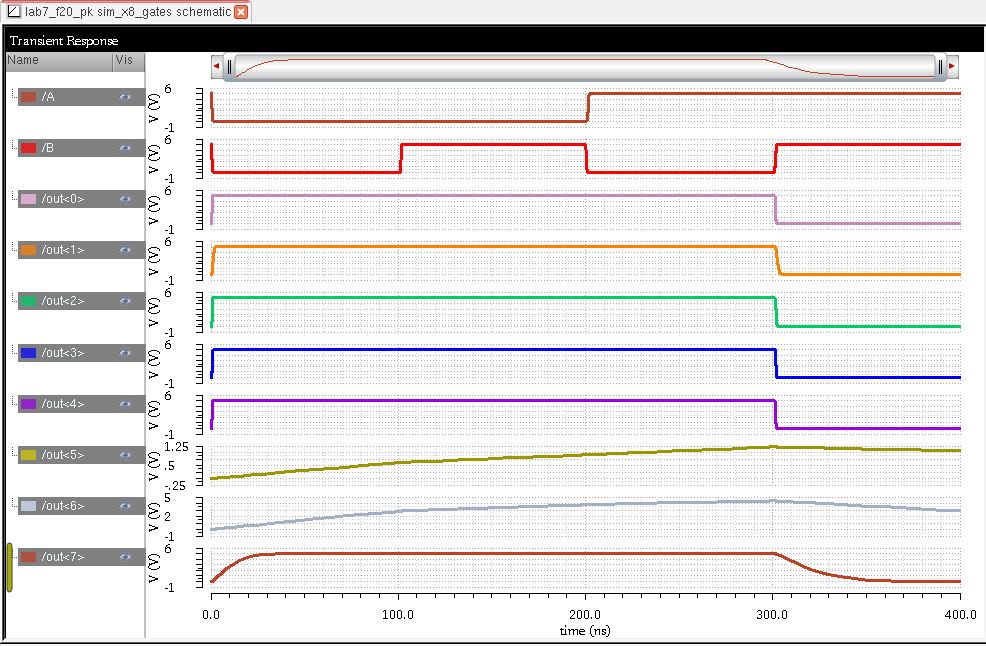
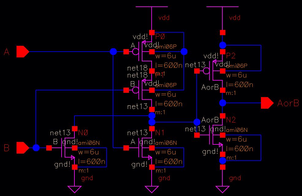
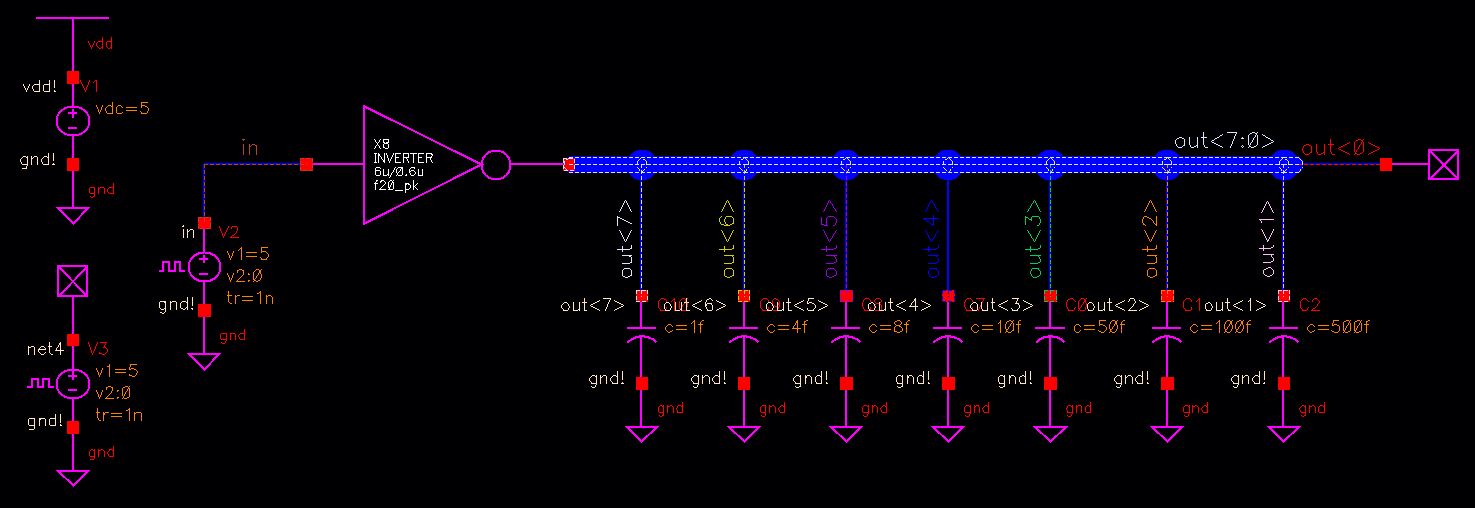
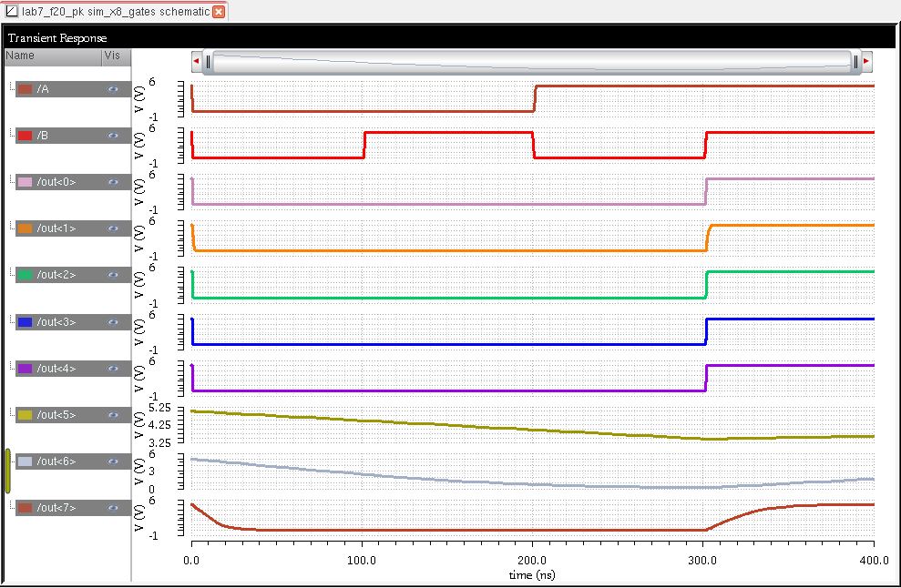
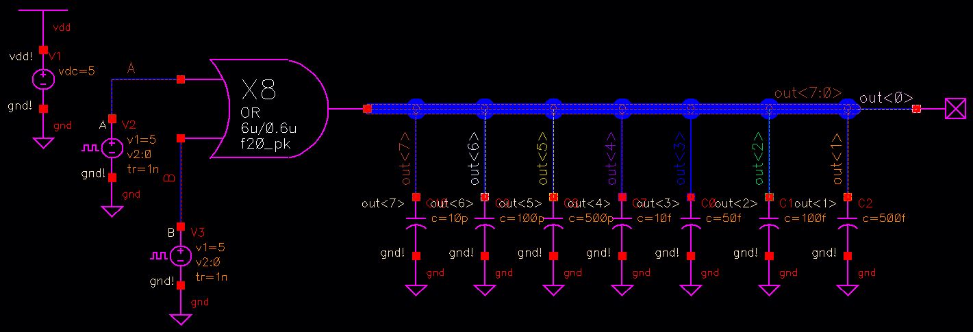
Schematic and simulation plot for 8-bit OR gate:
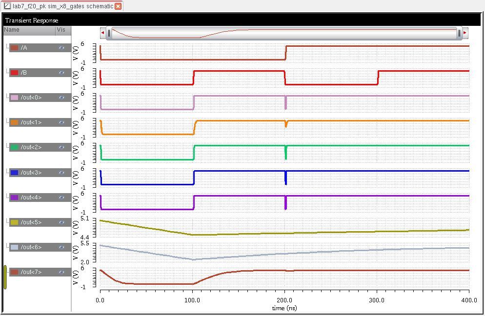
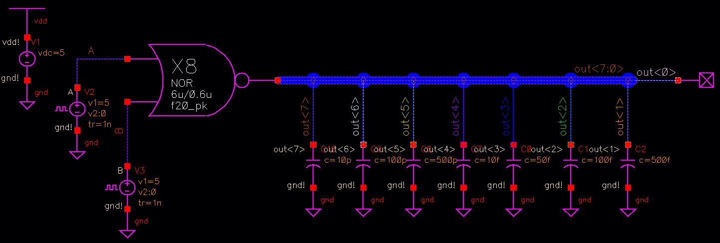
Schematic and simulation plot for 8-bit NOR gate:
- Examine and simulate the schematic of a 2-to-1 DEMUX/MUX.
Schematic and symbol view is seen below:


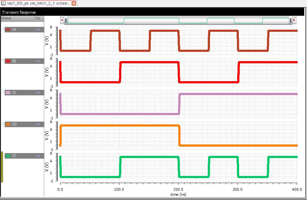
Schematic used for simulation:

Simulation results: MUX/DEMUX is comprised of pair of transmission gate (TG).
Transmission gate passes signal (bi-directional) when select is high.
The logic equation given for MUX/DEMUS is Z = A*S + B*Si.
From the simulations, we can see output Z follows corresponding select switch input (S or Si)
When S is high, Z follows A, and when Si is high, Z follows B.
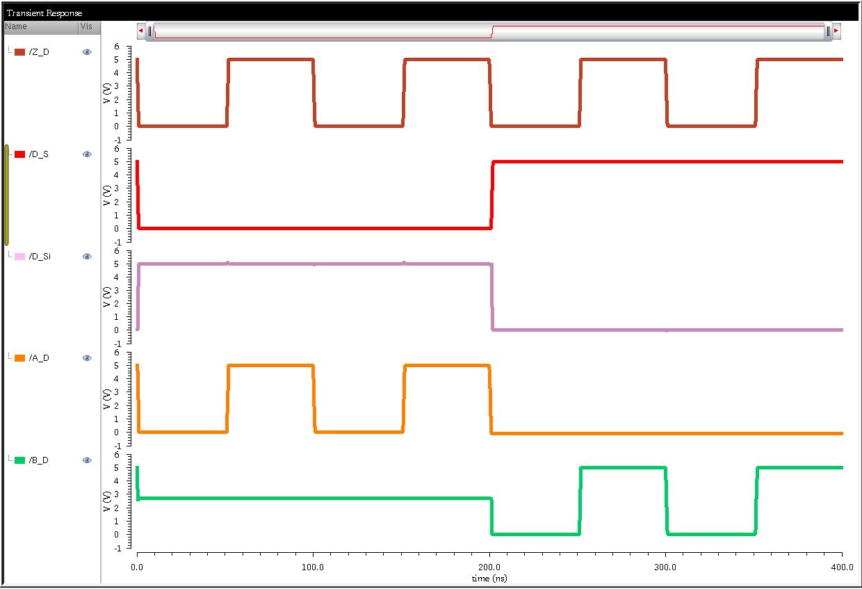
The logic equation for DEMUX can be written as A_D = D_Si * Z_D and B_D = D_S * Z_D (using input from schematic).
When D_Si is high, A_D follow Z_D, and when D_S is high, B_D follow Z_D.
- Create an 8-bit wide word 2-to-1 DEMUX/MUX schematic and symbol.
- Include an inverter in your design so the cell only
needs one select input, S (the complement, Si, is generated using an
inverter).
Schematic and symbol of 8-bit wide word 2-to-1 DEMUX/MUX is shown below:


- Verify the operation of design using simulations.
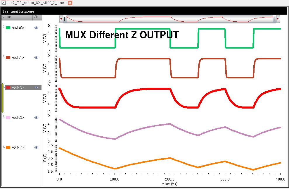
Schematic for simulating 8-bit MUX/DEMUX with selected outputs:

Simulation plot for 8-bit MUX: out<0> is same as output Z from plot above
(number of different outputs with different capacitive loads)
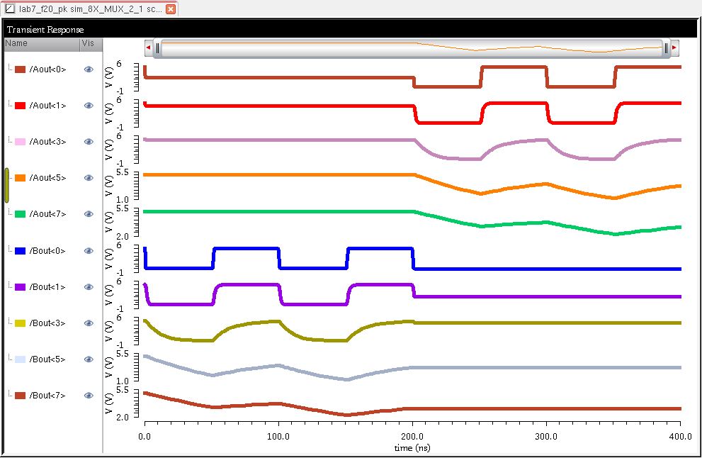
Simulation plot for 8-bit DEMUX: Aout<0> & Bout<0> are same as output A_D & B_D from plot above
(number of different outputs with different capacitive loads)
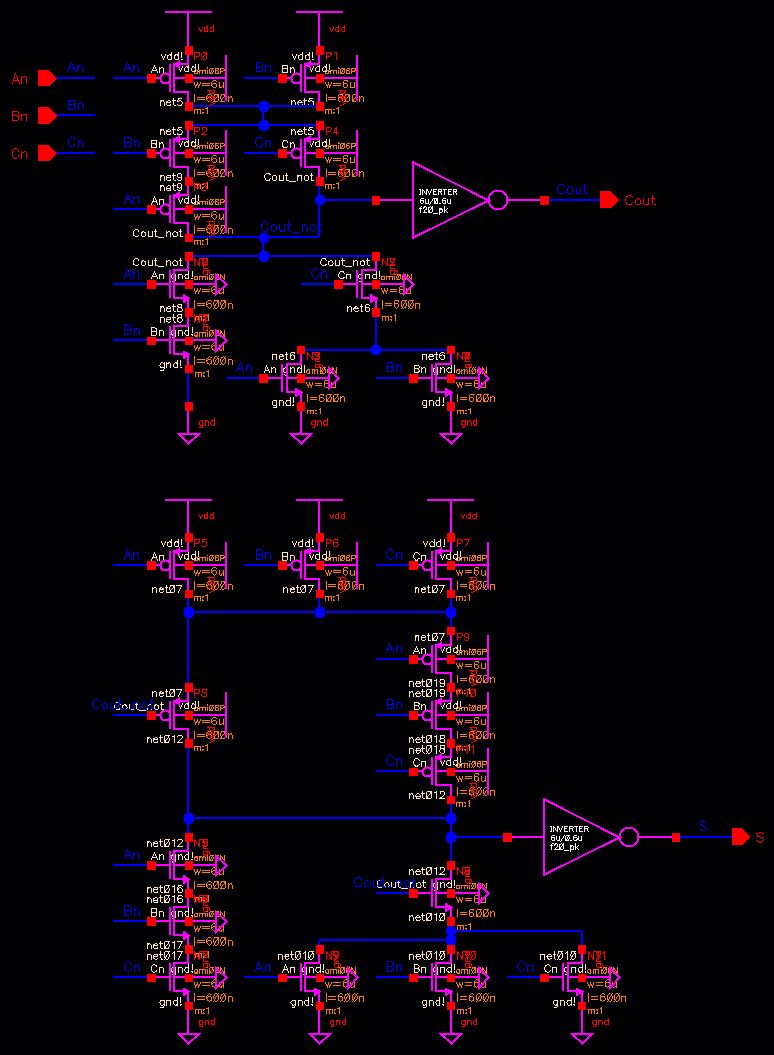
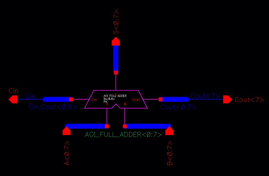
- Draft the schematic of the full-adder seen in Fig. 12.20 using 6u/0.6u devices (both PMOS and NMOS).
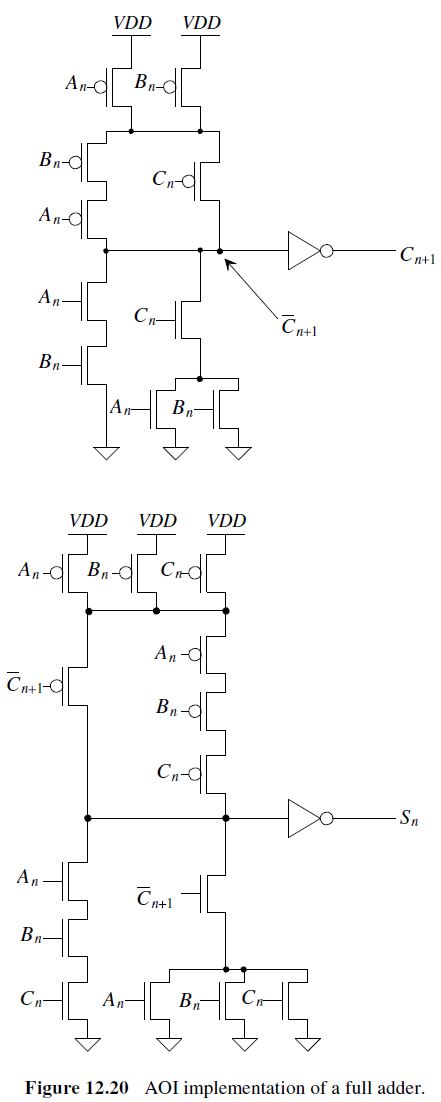
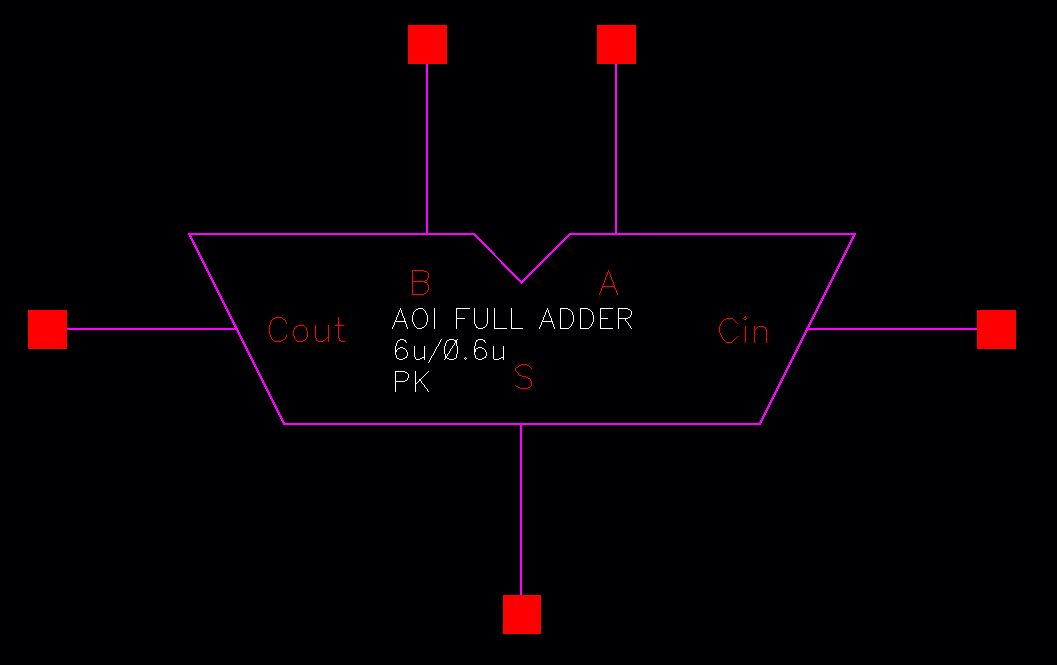
- Symbol for this circuit is seen below:
- Use this symbol to draft an 8-bit adder schematic and symbol.
Schematic and symbol for 8-bit adder is seen below:

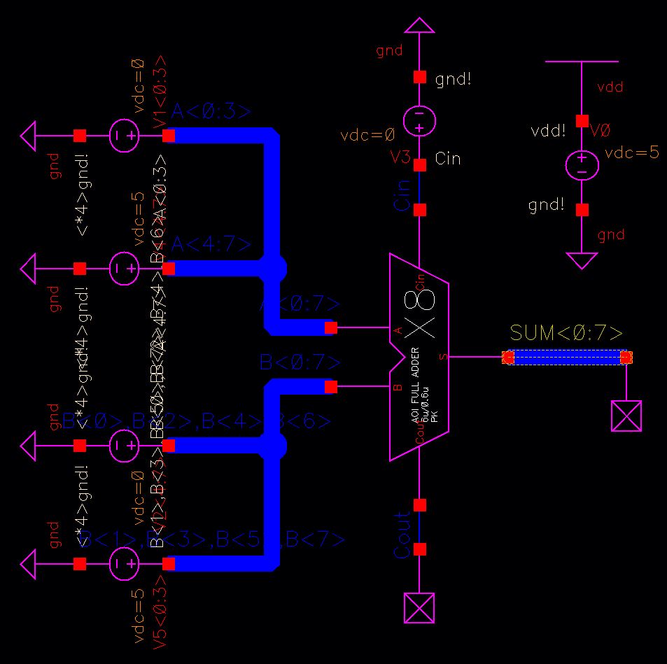
- Simulate this 8-bit adder cell
Schematic for simulation for input A & B of:
A = 00001111
B = 01010101
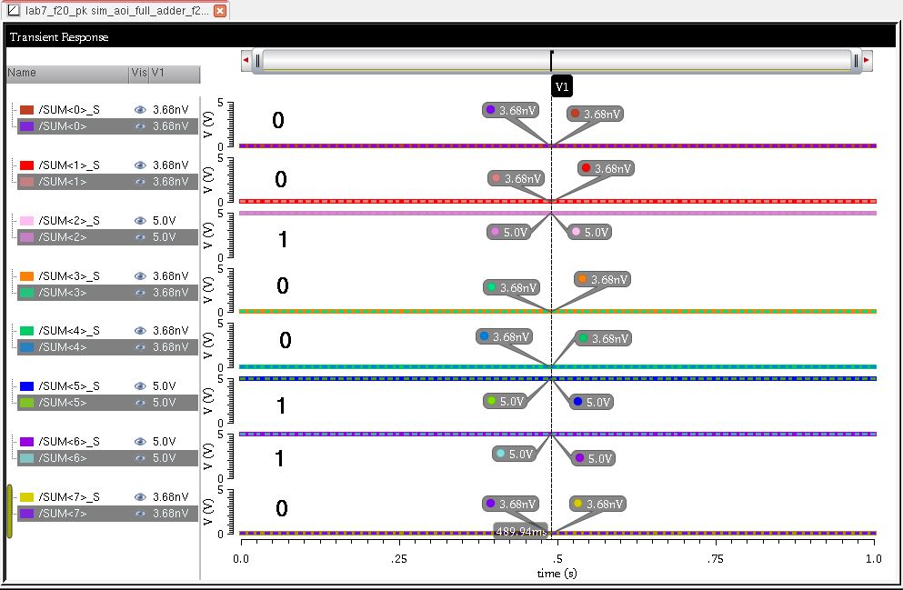
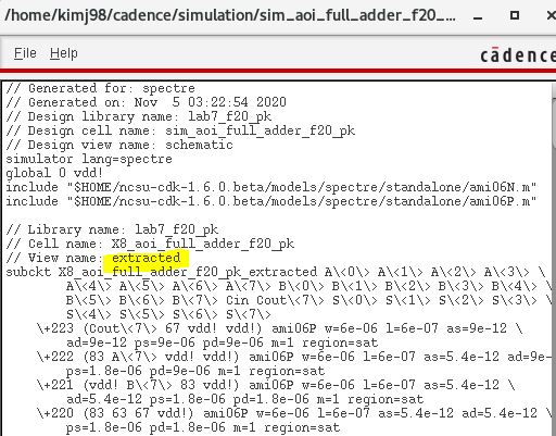
Simulation result (note: dotted lines represent extracted cell, confirms that my layout is working correctly)
A =00001111 (15)
B =01010101 (+85)
SUM =01100100 (100)
- Layout 8-bit adder cell, show your layout DRCs and LVSs with no errors.
- First, layout 1-bit full adder as a single cell to layout 8-bit adder.
Layout and extracted view shown below (click for a larger image):
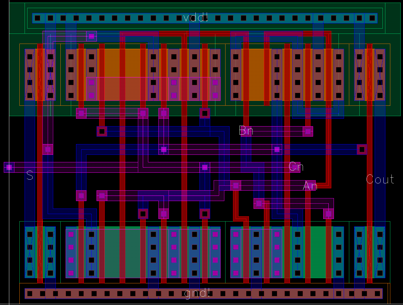

1-bit FULL ADDER cell DRC and LVS without error shown below:


- Using the 1-bit Full Adder cell above, layout 8-bit full adder.
Layout and extracted view shown below (click for a larger image) press shift and scroll to see pins:


8-bit FULL ADDER cell DRC and LVS without error shown below:


All work is back-up in google drive.
END of LAB 7
Return
to EE 421L
Labs