Lab
4 - EE 421L
Prelab:
- Back-up all of previous work.
- Read through the lab manual before starting it.
Schematic and IV curve of PMOS
Schematic and IV curve of PMOS from lab4.zip file
Lab Report:
Generate 4 schematics and simulations (using 6u/600n for NMOS, and 12u/600n for PMOS):
(1) ID vs. VDS of an NMOS device for VGS varying from 0V to 5V in 1V steps while VDS varying from 0V to 5V in 1mV steps.
First, create a schematic for ID vs. VDS plot seen below:

Launch ADE-L and set-up simulation: set-up model library to include our model
Simulation result of ID vs. VDS seen below:

(2) ID vs. VGS of an NMOS device for VDS = 100mV where VGS varying from 0V to 2V in 1mV steps.
Schematic for ID vs. VGS is seen below:

set up analyses as seen below:
Simulation of ID vs. VGS seen below:
From the simulations, we know the threshold voltage of NMOS is about 850 mV.

(3) ID vs. VSD of a PMOS device for VSG varying from 0V to 5V in 1V steps while VSD varying from 0V to 5V in 1mV steps.
Schematic for ID vs. VSD is seen below:

set up analyses as seen below:
Simulation of ID vs. VSD seen below:

(4) ID vs. VSG of a PMOS device for VSD = 100mV where VSG varying from 0V to 2V in 1mV steps.
Schematic for ID vs. VSG is seen below:

set up analyses as seen below:
Simulation of ID vs. VSG seen below:

Layout a 6u/600n NMOS device and connect all 4 MOSFET terminals to probe pads.
Probe pad schemtic, symbol and layout:
For creating a probe pad, follow first part of tutorial 6.
the difference is the size for metal 3 and glass layers.
(refer to design rule below for reference)
First create a schematic with pin named probe_pad
add a no_conn to avoid errors and create a corresponding symbol as see below:


we can set the minimum width and length of 30 um,
however, the minimum passivation opening is 20 um,
and 20 um does not fall into our grid of 1/2 lambda.
Therefore, adjust the passivation opening to 22.6 um
and metal 3 layer to 33.6 um to keep overlap passivation of 6um.

- Create a schematic and create a corresponding symbol for NMOS seen below:


- Create a schematic with probe pad and create a corresponding symbol seen below:
(schematic will be used for LVS and symbol will be used for simulations)


-Layout NMOS with probe pads:
In order to minimize debugging time for DRC,
First, instantiate 4 probe pads and set them 30 um away from each other (run DRC)
and layout 6u/600n NMOS, use ruler to minimize distance between pads and NMOS (run DRC)
add metal wires to complete the layout (run DRC)
run DRC often to minimize time for debugging the errors.
Completed NMOS layout seen below:
(click on the image to view the layout in full detail)
Run DRC for errors
Run LVS
Run simulation to verify my layout
(running simulation using the probe symbol in a schematic and use extracted view)

(simulation result confimed my layout is working correctly)

Layout a 12u/600n PMOS device and connect all 4 MOSFET terminals to probe pads.
- Follow the same procedure as above
Create a schematic and a symbol for basic PMOS with size of 12u/600n


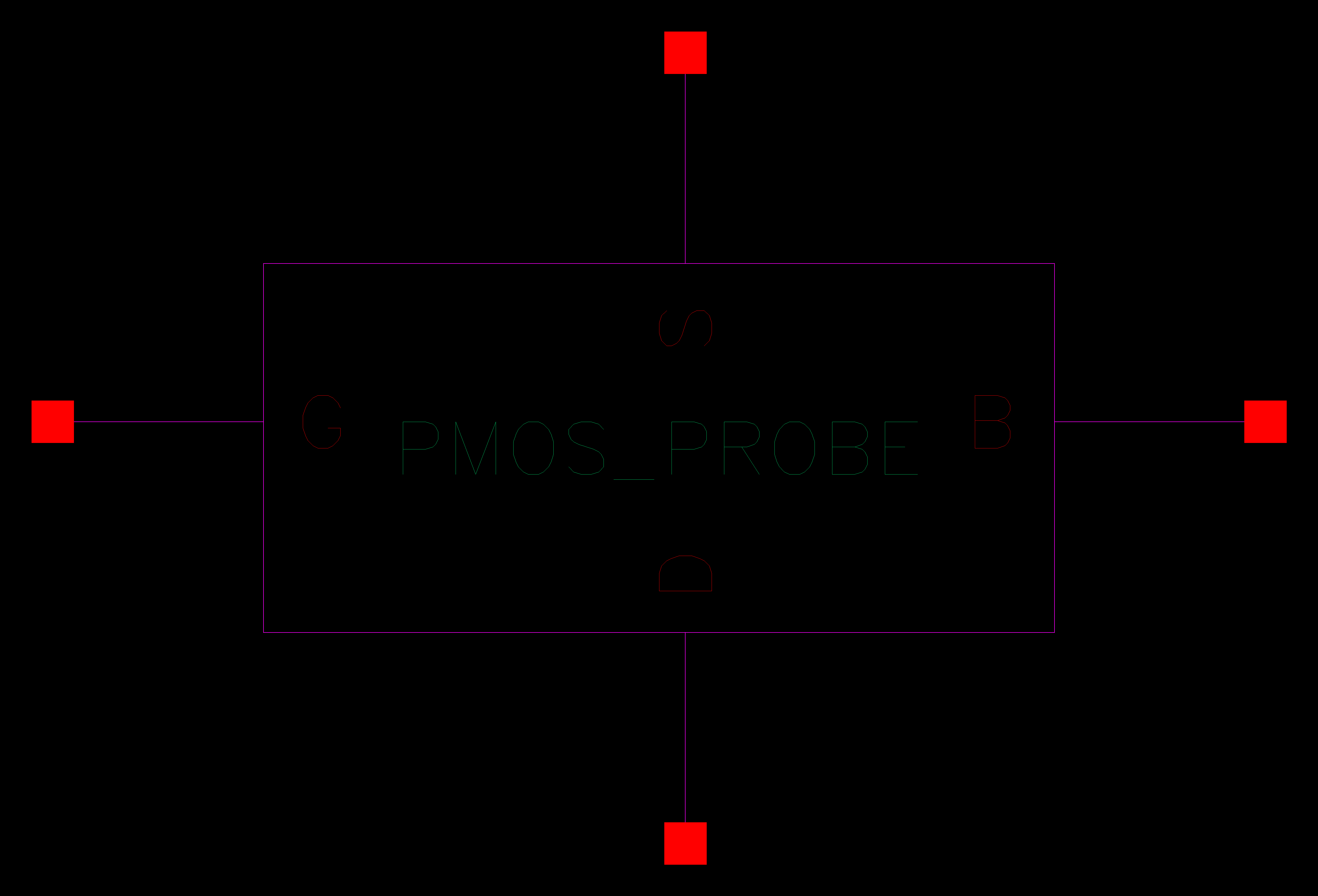
Create a schematic and a symbol for PMOS with probe pads


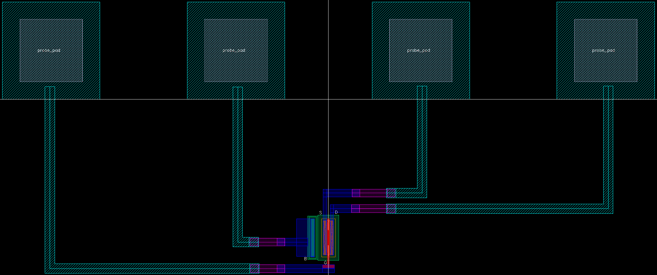
Layout of PMOS with probe (run DRC & LVS)
Completed NMOS layout seen below:
(click on the image to view the layout in full detail)
run DRC & LVS
Verify layout using simulation

(simulation result confimed that my layout is working correctly)

Make sure to back up all work
End of LAB4

