Email: alvara6@unlv.nevada.edu
October 7,
2020
Lab
Description
·
Design, layout, and simulation of a CMOS
inverter
Pre - Lab
- Back-up
all of your work from the lab and the course.
- Go
through Tutorial 3
seen here.
Backing
up previous lab work
All of my previous work has been
backed up as after every lab we are required to back up our assignments and
work. 
Tutorial
3
Design of the CMOS inverter. Firstly,
here are the schematics for that of a CMOS inverter. A CMOS inverter consists
if a PMOS and NMOS transistor. From the initial schematic we make a inverter symbol.


Secondly, we
have to create the layout of the inverter. The first image in this section is
the layout, the second image in this section is a layout with the editor view
from 0 to 0 layers.
The next image
in this section is the extracted view of the CMOS inverter.


LVS menu and
snip showing that the netlists match.


Schematic with
symbol

Simulation of
the CMOS inverter in which we see that if the input is high then the output is
low and if the input is low then the output is high.

Simulation by
changing environment and simulating the extracted view.

Lab Tasks
·
Draft schematics, layouts, and symbols for two inverters having
sizes of:
- 12u/6u (= width of the PMOS / width of the NMOS with
both devices having minimum lengths of 0.6u)
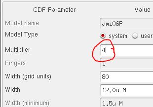
- 48u/24u where the devices use a multiplier, M = 4 (set
along with the width and length of the MOSFET, image), as
seen below
o
Using SPICE simulate the
operation of both of your inverters showing each driving a 100 fF, 1 pF, 10 pF, and 100 pF capacitive load
- Comment, in your
report, on the results
- Use UltraSim
(Cadence's fast SPICE simulator for larger circuits at the cost of
accuracy) and repeat the above simulations
Lab
Schematic of 12u wide PMOS and 6u wide NMOS.
Notice that
the schematic has two pins which are A and AI while the layout has four pins
which are A, Ai, vdd!, and gnd!.


Layout and
Extracted view of 12u wide PMOS and 6u wide NMOS


DRC showing
zero errors and netlists matching.


Schematic of 48u wide PMOS and 24u wide NMOS
An important note
is that this schematic looks like the one above except the fact that this schematic
has m = 4. This means the original values will
Be multiplied
by 4. Again notice that the schematic has
two pins which are A and AI while the layout has four pins which are A, Ai, vdd!, and
gnd!.


Layout and
Extracted view of 48u wide PMOS and 24u wide NMOS


DRC showing
zero errors and netlists matching.


Simulations of 12u wide PMOS and 6u wide NMOS

Spectre of 12u wide PMOS and 6u wide NMOS

UltraSim of 12u wide PMOS and 6u wide NMOS

In this lab we were supposed to use both ultrasim and spectre. Ultrasim is
faster than spectre and is useful for larger circuits but the fast speed comes
at the cost of accruacy. Since this is not a large or complicated circuit the
results are fairly similar.
As expected the inverter goes low when the input is high and vice versa. As
capacitor values is increased the longer
it takes to charge and discharge the circuit. The 100pf is ouputting the same
value as the input which means the inverter cannot handle this value. The 100fF
and 1pF capacitors work correctly, but the 10pF is in between and maybe should
not be used.
Simulations of 48u wide PMOS and 24u wide NMOS

Spectre of 48u wide PMOS and 24u wide NMOS

UltraSim of 48u wide PMOS and 24u wide NMOS

What was noticed about multiplying the inverter by four is that the
inverter can handle the capapcitor values better. For example the 100fF and the
1pF capacitor output are more quickly inverted, for the 10pF capacitor it makes
it more relaible because now it is being drawn to the inverted value instead of
being in between like the previous schmatic and simulations. As for the 100pF
it still is not the correct inverted value but it at least is not the same value
as the input so maybe if we have a higher multiplier than maybe this capacitor
will work.
Backing Up Work


As seen by the snips
above these were the steps that I used to back up my work. First, I found the
tutorial folder in my CMOSedu folder in the MobaXTerm.
After finding where
the folder was, I downloaded the folder to the desktop and later sent it to a
compressed zipped folder.
After making a ZIP
file I uploaded them to my google drive with the date in the
title. This should complete my backup process. This will be the
process I use in the future.
This concludes Lab 5.