Lab Project - EE 421 Digital Integrated Circuit Design
Authored
by Moriah Wingrove
Email: wingrove@unlv.nevada.edu
Due: Nov 13 2019
Project Description:
Project
(not a group effort, each student will turn in their own project) –
design a circuit that takes a 9-11 MHz clock signal and generates
a
36-44 MHz clock signal. In other words, design x4 clock multiplier. The
input clock is multiplied by 4 and output. Assume the input clock
signal has a 50% duty cycle.
NOVEMBER 13:
- First
half of the project (schematics and design discussions) of your design
and an html report detailing operation (including simulations), is due at the beginning of lab on Nov. 13.
- Your design report in html should show various input clock frequencies and VDD voltages to show it works.
- Put your report (proj.htm) in a folder called /proj in your directory at CMOSedu and link to your index.htm page.
- Dr. Baker will go over your design with you (in person), including running simulations, when lab meets on Nov. 13.
NOVEMBER 20:
- Second half of the project, a verified layout and documention (in html), is due at the beginning of lab on Nov. 20.
- Dr.
Baker will meet with you on Nov. 20 to go over your layout and,
again, put your report in the /proj folder in your directory at
CMOSedu.
- Ensure that there is a link on your project report webpage to your zipped design directory.
Schematics and Design Discussion:
INVERTER - 12u/6u min length:
A
12u/6u inverter (with minimum lengths - 0.6u) was used to square up the
output of the delays and both XOR gates. The PMOS was chosen to have
twice the width of the NMOS so the resistance of the PMOS and NMOS were
the same to ensure vsp ~ vdd/2.


INVERTER - 12.6u/6u long length 12.6u:
In
order to increase the delay of the inverter the lengths of both the
NMOS and PMOS were increased to 12.6u. This was chosen over using
capacitors inbetween inverters to help reduce the size of the layout.


INVERTER - 12u/6u long length 10.2u:


XOR gate:
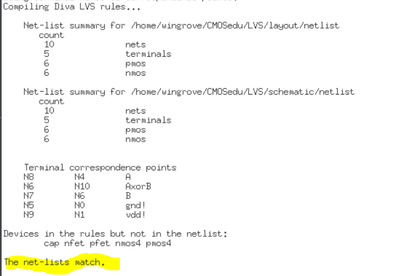
The XOR gate used in this design is the same one created from lab 6. All of the MOSFET devices in the XOR gate are 6u/600n.
schemetic of XOR gate using PMOS and NMOS devices

Logic symbol of XOR gate

Schematic used to simulate XOR gate to ensure the gate performed as expected

Truth table for a 2-input XOR gate

It
is observed from the simulation above that the XOR gate does operate
correctly. There can be errors in the gate as seen above that are
caused by the rise/fall times of the input signals. In the XOR output
above there is a glitch in the signal that is due to the falling edge
of input B as it goes to 0 and the rising edge of input A as it goes
from 0 to 5V. Both signals are a logic 0 for a brief peroid of time
causing the output of the XOR gate to go to 0V.
Design:
The
purpose of this project was to take a 9-11MHz clock signal and generate
a 36-44MHz clock signal. The input clock signal has a 50% duty cycle.
It
was chosen that the 36-44MHz clock cycle generated would have a duty
cycle of approximately 50%. In order to generate the necessary clock
cycle two XOR gates were used with two different delays. The
inputs to the first XOR gate would be the original 9-11MHz clock
signal and the delayed 9-11MHz signal in order to generate a 18-22MHz
clock signal. The inputs to the second XOR gate are the 18-22MHz signal
and the delayed 18-22MHz signal.
An input clock cycle of
10MHz was used to create both delays needed due to the fact that 10MHz
is the middle frequency between 9-11MHz.
Using f = 10MHz, the
period of the input signal was calculated to be 100ns. The input signal
has a 50% DC so the signal is on for 50ns and off for 50ns. The first
delay created would need to be for 25ns and the second delay was 12.5ns.
Delay 25ns:
The lengths on the long inverter were chosen to be 12.6u which is 21 times the minimum length
tpLH = 0.7(40000)(12.6/12.6)(2.5f*12.6(12.6+6))
=0.7(40000)(1)(586f)
= 16.4ns
tpHL= 0.7(20000)(12.6/6)(2.5f*12.6(12.6+6))
=0.7(20000)(2.1)(586f)
= 17.23ns
The expected delay from the inverter with length 12.6u was 33ns


Delay 13ns:
An
20/10 inverter with minimun length was placed in front of the long
inverter on the 13ns delay in order to help sqaure up the input signal
from the first XOR gate. The lengths on the long inverter were chosen
to be 17 times the minimum length.
tpHL = tpLH = 0.7(40000)(10.2/12)(2.5f*10.2(12+6))
=0.7(40000)(0.85)(459f)
= 10.924ns
The expected delay from the inverter with length 10.2u was 10.92ns


The total delay from the 13ns delay schematic was measured to be 19.67ns with tpLH = 11.31ns and tpLH = 8.36ns
Design of x4 clock multiplier


Testing & Simulations:
Test ONE: f = 10MHz, T = 100ns, Vdd = 5V, Vpulse = 0V-5V
The x4 clock multiplier was designed to take a 10MHz input signal and generate a 40MHz signal at 5V


The output period is 50.91972ns - 26.22198ns = 24.69774ns
The output frequency = 1/T
fout = 1/24.6977ns
fout = 40.49MHz
the output frequency of 40.49MHz is close to the expected 40MHz value
Test TWO: f = 9MHz, T = 111.11ns, Vdd = 5V, Vpulse = 0V-5V tr = 100ps -- fout = 33MHz


Increasing
the rise/fall times of the input signal causes a shorter period on the
output of the x4 clock. The signal takes a lot longer to rise which
means the edges are not smooth and there is less distance between the
falling egde of the input and rising edge of the delayed input.
Test Three: f = 11MHz, T = 90.91ns, Vdd = 7V, Vpulse = 0V-7V tr = 100ps -- fout = 36MHz


When
Vdd is increased along with the input voltage the amplitude of the
output signals is increased to vdd as well. The output of the x4 clock
is higher in amplitude and the period becomes more narrow than if vdd
had been left at 5V. If vdd were to be decreased below 5V then the
amplitude of the output signal would decrease and the period would be
wider. Since the XOR gate is being used as an edge detector if vdd is
too low and the signal is not fast enough glitches can be observed in
the output of the x4 clock.
Test Four: f = 11MHz, T = 90.91ns, Vdd = 4V, Vpulse = 0V-4V tr = 1ps --


PART TWO: LAYOUT
1) LAYOUT - 12u/6u Inverter
The
layout for the 12u/6u inverter using a minimun length of 0.6u is the
same one created from lab. The layout was copied into the project
design directory and used again.
LAYOUT VIEW
DRC RESULTS


The
layout was extracted after passing the design rule check (DRC). The
extracted layout was then compared to the schematic using the LVS tool.
Below are the extracted view of the 12u/6u inverter, the LVS results,
and the netlist comparison obtained from the output of the LVS.
EXTRACTED
VIEW
LVS RESULTS
NETLIST


2) LAYOUT - Inverter 12u/6u long length L = 12.6u
The
layout for the inverter used to create the 25ns delay was implemented
using the layouts for a PMOS and NMOS with long lengths. The PMOS used
was a 12.6u/12.6u and the NMOS was 6u/12.6u. In order to be consistent
the inverter was laid out in a similar manner to that of the 12u/6u
inverter pictured above.
LAYOUT VIEW
DRC RESULTS


The
layout was extracted after passing the design rule check (DRC). The
extracted layout was then compared to the schematic using the LVS tool.
Below are the extracted view of the 12u/6u inverter using L = 12.6u, the LVS results,
and the netlist comparison obtained from the output of the LVS.
EXTRACTED
VIEW
LVS RESULTS
NETLIST


3) LAYOUT - Inverter 12u/6u long length L = 10.2u
The layout of the 12u/6u inverter with length L = 10.2u was created using a 12u/10.2u PMOS and 6u/10.2u NMOS
LAYOUT VIEW
DRC RESULTS


The
layout was extracted after being evaluated for design violations. The
extracted layout was then compared to the schematic using the LVS tool.
Below are the extracted view of the 12u/6u inverter using L = 10.2u, the LVS results,
and the netlist comparison obtained from the output of the LVS.
EXTRACTED
VIEW
LVS RESULTS
NETLIST


4) LAYOUT - Delay of 25ns
The
layout of the 25ns delay was made by combining three of the 12.6u/6u
long length inverters in series with each other. Once those inverters
were properly connected they were combined in series with three 12u/6u
inverters. There are 6 inverters connected in series with each other.
The three long length inverters were placed first in order to create
the desired delay. After the desired delay had been achieved three
ideal 20/10 inverters were placed at the end of the chain in order to
ensure the output signal had fast edges.
Click images for a larger picture.
LAYOUT VIEW
DRC RESULTS 

The
layout was extracted after being evaluated for design violations. The
extracted layout was then compared to the schematic using the LVS tool.
Below are the extracted view of the 25ns delay, the LVS results,
and the netlist comparison obtained from the output of the LVS.
EXTRACTED
VIEW
LVS
RESULTS


NETLIST

5) LAYOUT - Delay of 12.5ns
The
layout of the 12.5ns delay was made by placing a 12u/6u inverter at the
beginning of the layout. After the first inverter had been placed it
was connected in series with two 12u/6u
long length, L = 10.2uinverters connected in series. After the desired
delay had been laid out another 12u/6u inverter was placed in series at
the end in order to clean up the output signal. The 12u/6u inverter at
the end sharpens the edges of the output by making the rising/falling
edges of the signal faster.
Click images for a larger picture.
LAYOUT
VIEW
DRC RESULTS


The
layout was extracted after being evaluated for design violations. The
extracted layout was then compared to the schematic using the LVS tool.
Below are the extracted view of the 12.5ns delay, the LVS results,
and the netlist comparison obtained from the output of the LVS.
EXTRACTED
VIEW
LVS
RESULTS


NELTIST

6) LAYOUT - XOR Gate
The layout of the XOR gate is the same layout as from lab 6. The layout was copied into the project
design directory and used again.
LAYOUT
VIEW
DRC RESULTS


The
layout was extracted after being evaluated for design violations. The
extracted layout was then compared to the schematic using the LVS tool.
Below are the extracted view of the XOR gate, the LVS results,
and the netlist comparison obtained from the output of the LVS.
EXTRACTED
VIEW
LVS
RESULTS

NETLIST
7) LAYOUT - x4 Clock Multiplier
For
the layout of the x4 clock multiplier the components were placed
end-to-end so that the individul power and ground connections (vdd! and
gnd!) were routed together. The input to the x4 clock multiplier was
connected to the input of the 25ns delay as well as one of the first
XOR gate inputs (XOR1) . The output of the 25ns delay was connected
into the other input of the XOR1 gate in order to obtain the delayed
input needed to generate the x2 clock signal. The output of XOR1 was
fed into one of the inputs of the second XOR gate (XOR2) as well as
into the input of the 12.5ns delay. A pin named output was connected on
the output of XOR2 for the output of the x4 clock multiplier.
Click images for larger view
LAYOUT
VIEW
DRC RESULTS


Zoomed x4 clock multiplier - input pin
Zoomed x4 clock
multiplier - output pin


The
layout was extracted after being evaluated for design violations. The
extracted layout was then compared to the schematic using the LVS tool.
Below are the extracted view of the x4 clock multiplier and the LVS results.
EXTRACTED VIEW

LVS RESULTS
NETLIST


Project Directory:
Return to my labs:
Return to EE 421 labs: