Lab 8 - EE 421L
Authored
by: Steve Salazar Rivas, Adrian Angelo G. Fuerte, & John Patrick Buen
Email: salazs3@unlv.nevada.edu
fuerta1@unlv.nevada.edu
buenj1@unlv.nevada.edu
December 3, 2019
Zipped-up directory: Chip5_f19
Prelab: For lab 8, we went through Tutorial 6 in order to learn about the design and layout of a padframe for fabrication, and how to place circuit layouts in a padframe for fabrication.
| Layout Pad | 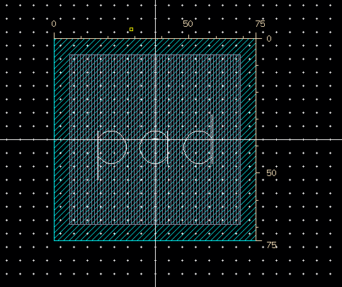 |
Layout
Padframe | 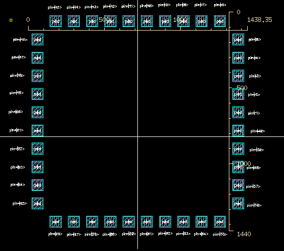 |
| Padframe Symbol | 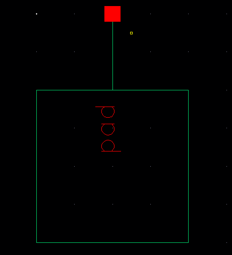 |
Lab Description:
For
the lab, we formed a group of three students to work on
this project. Our group consisted of John Patrick Buen, Steve Salazar,
and Adrian Fuerte.
As a group, we will be placing our circuits on a chip that will be tested once it is fabricated.
The following chip will include the following:
-One or more course project (in this case the Boost SPS)
-A 31-stage ring oscillator witha buffer for driving a 20pF off-chip load
-NAND and NOR gates using 6u/0.6u (W/L) NMOS and PMOS devices
-Transistors,
both PMOS and NMOS, measuring 6u/0.6u where all four terminals of each
device are connected to bond pads (7pads + common ground pad)
-Only one pad will be needed for the common ground
-25k resistor laid out below and a 10k resistor implement a voltage divider
| Schematics | Connections | Pin Names |
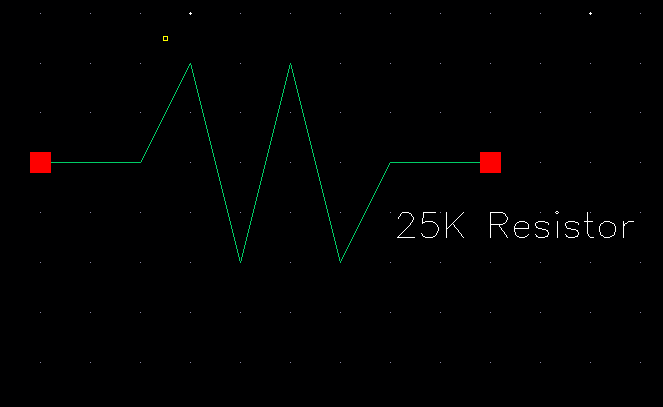
25k Resistor |
|
|
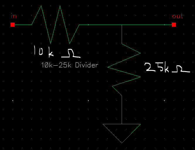
10k-25k Voltage Divider |
|
|
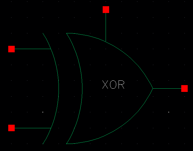
XOR Gate |
|
|
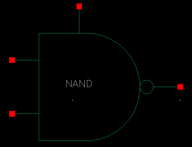
NAND Gate |
|
|
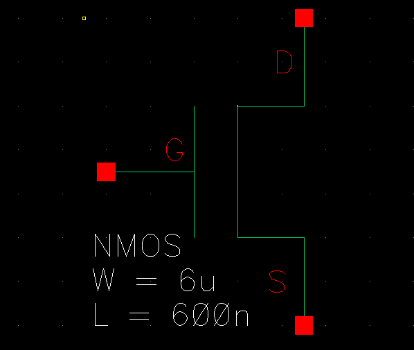
NMOS |
|
|
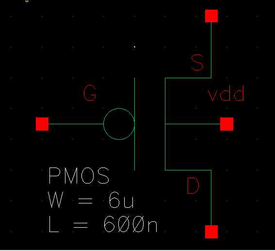
PMOS |
|
|
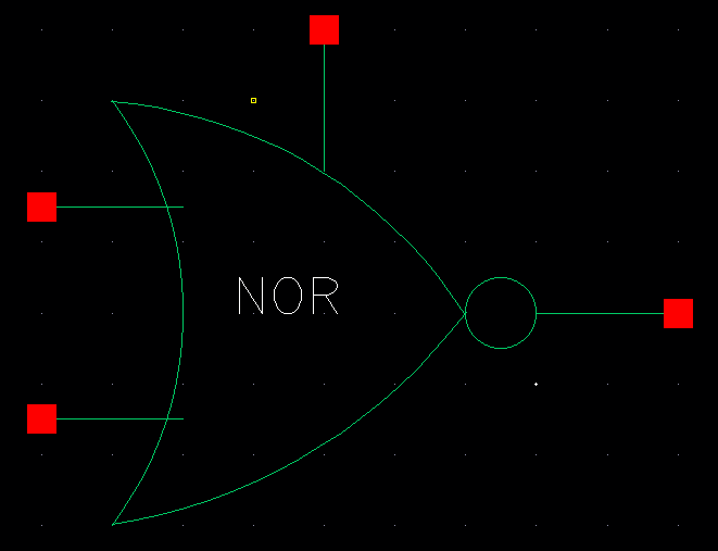
NOR Gate |
|
|
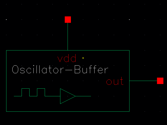
Oscillator Buffer |
|
|
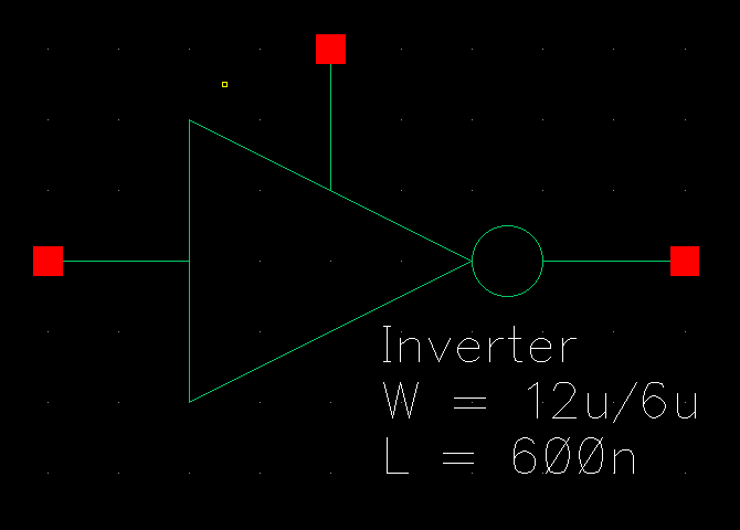
Inverter |
|
|
Pins not used for our components in our overall padframe...
Putting all of our components onto our padframe...
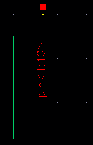
Overall padframe symbol |
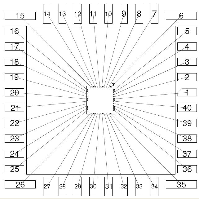
Pin numbering on padframe
|
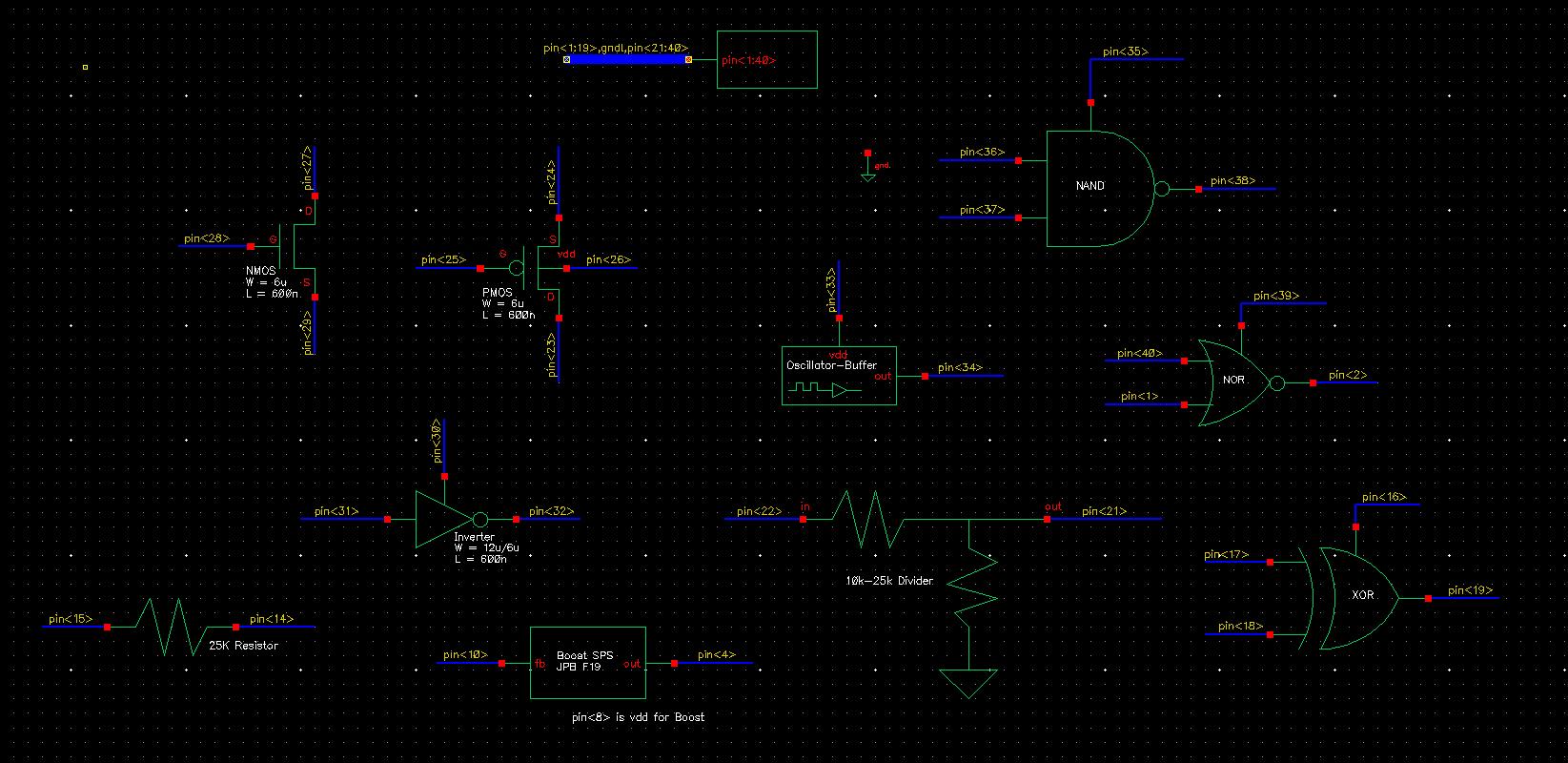
Schematic view of all the components connected onto the padframe |
Final padframe layout
|
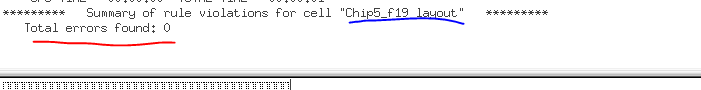
Our final padframe layout underwent DRC nicely | 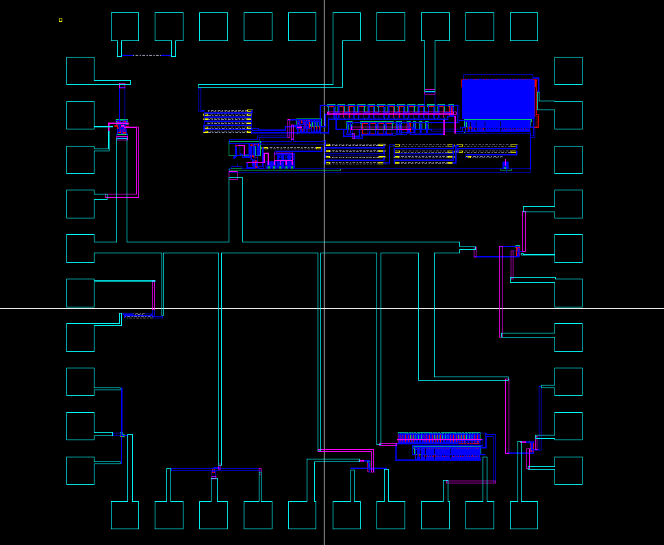
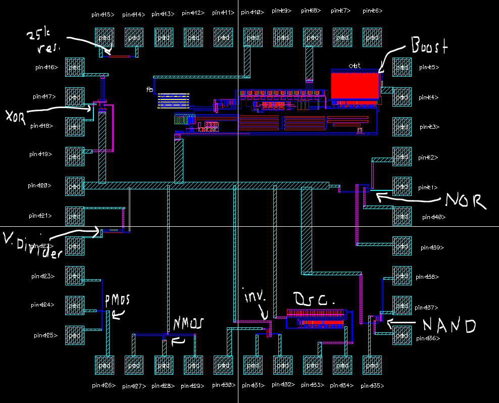
Extracted view of our final padframe |
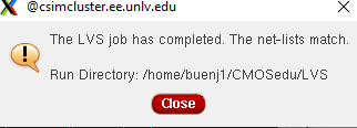
The overall padframe layout with all of our components connected to their respective pins underwent LVS quite nicely | 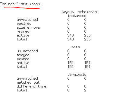
This is another verification of our net lists matching after undergoing LVS |
In order to test our chip, we would need several off chip components...
- Boost SPS
- Inductor
- Schottky Diode
- Capacitor
- Load
- A power supply is needed to power the device with a range from 3.75V to 5.25V
This concludes Lab 8 (Chip5_f19).
Return to EE 421L Labs