Lab 4 - EE 421L
Authored
by Steve Salazar Rivas
Email: salazs3@unlv.nevada.edu
September 25, 2019
Prelab: For lab 4, we went through Tutorial 2 to make an NMOS and a PMOS schematic and their respective layouts.
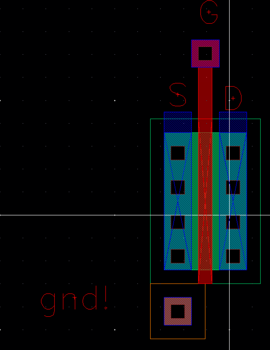
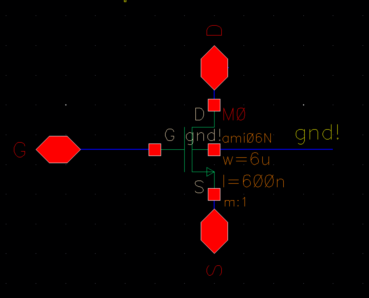
NMOS Layout and its respective schematic


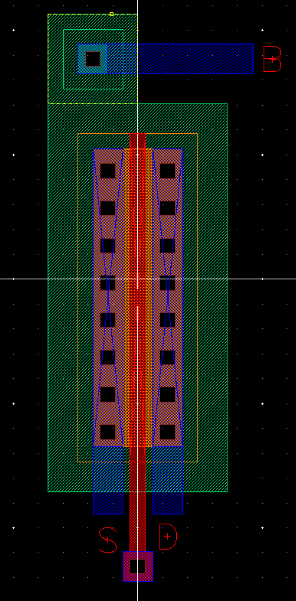
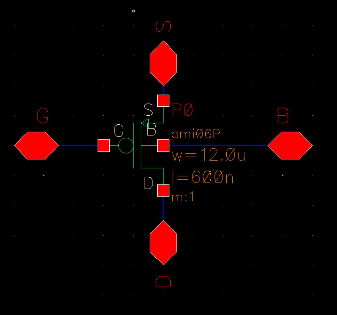
PMOS Layout with its respective schematic
Postlab:
For lab 4, we have to create four schematics and simulations and a
layout of an NMOS and PMOS device, respectively. We are also creating a
probe pad layout that will be connected to the terminals of the
MOSFETs.
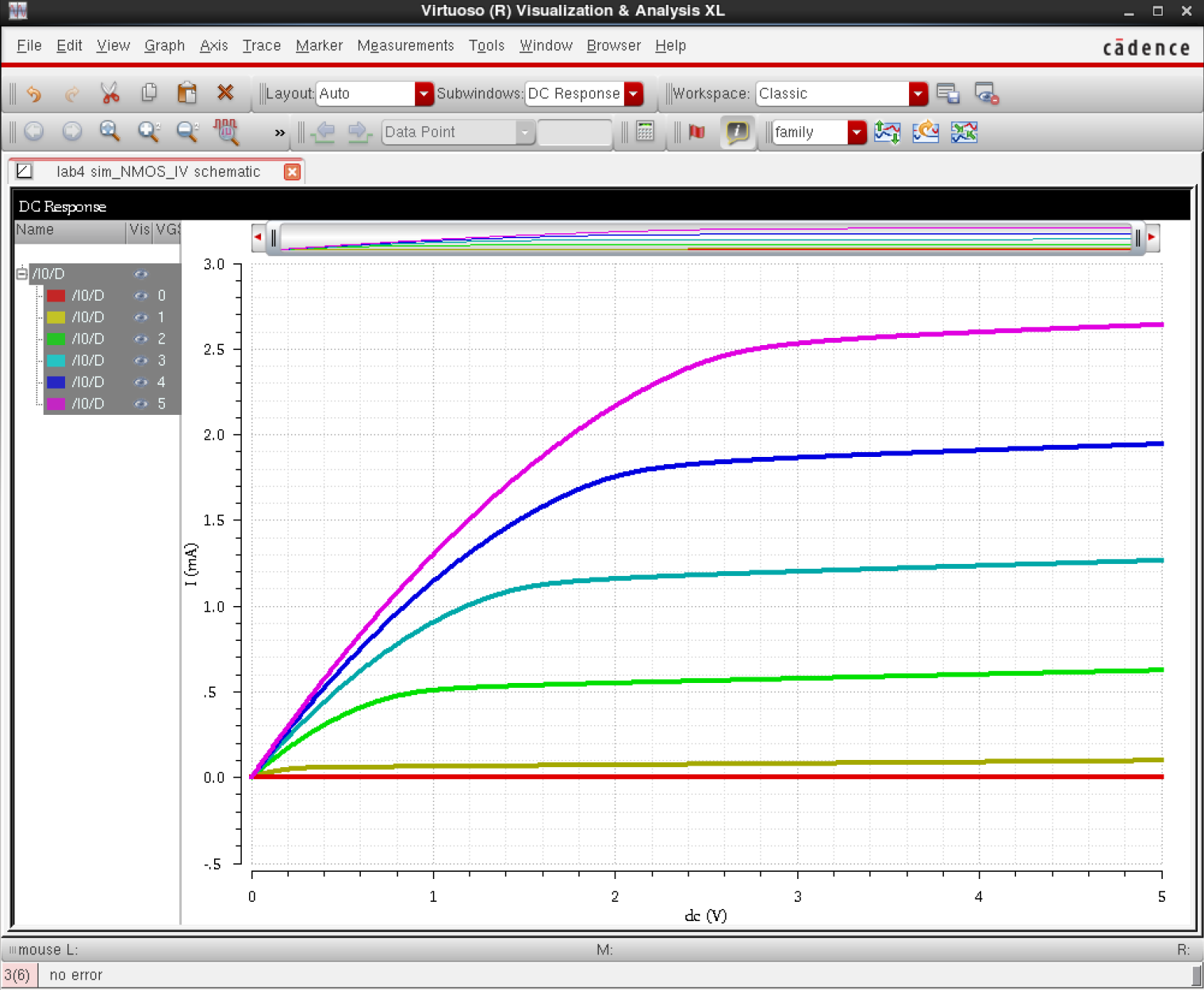
NMOS (ID v. VDS)
The
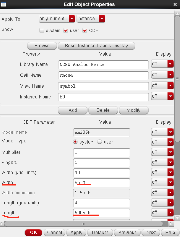
first part of lab 4 is creating an NMOS device with a 6u/600n
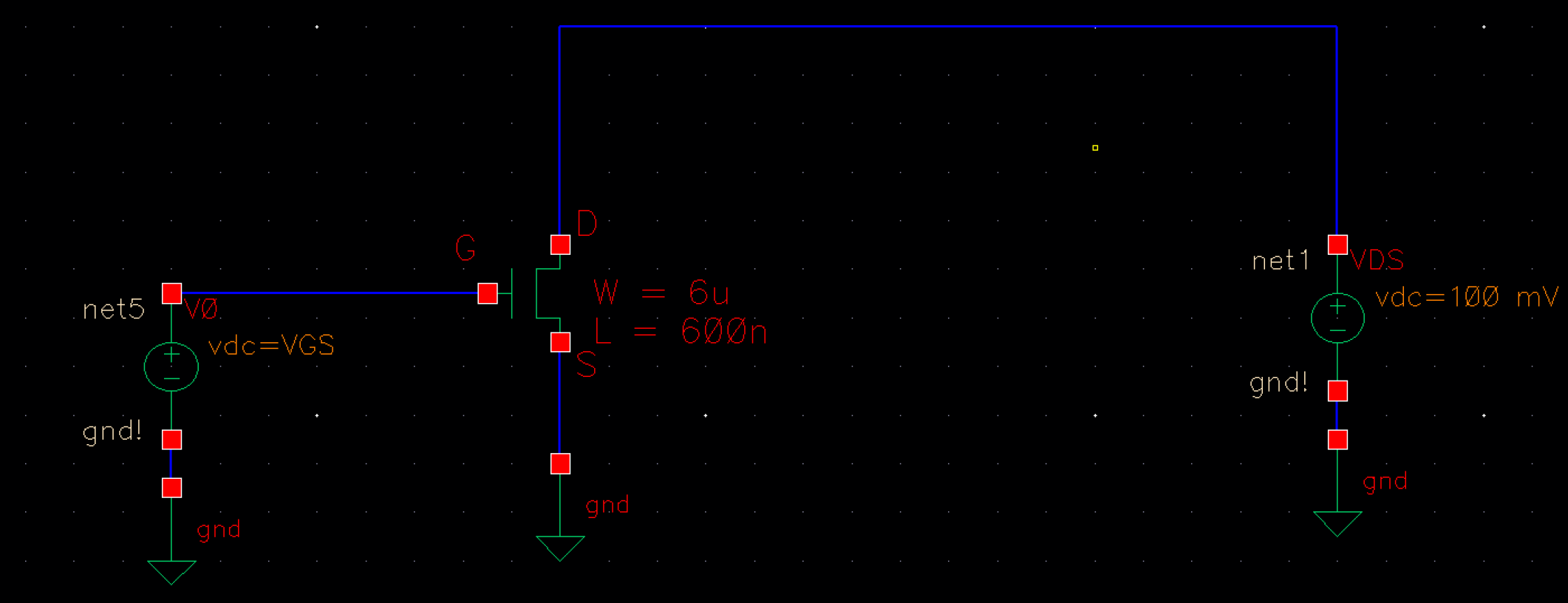
width-to-length ratio. The schematic created below will be simulated
for ID v. VDS for a VGS varying from 0 to 5V in 1V steps while VDS
varies from 0 to 5V in 1mV steps.We created a symbol for the NMOS as well (seen below).
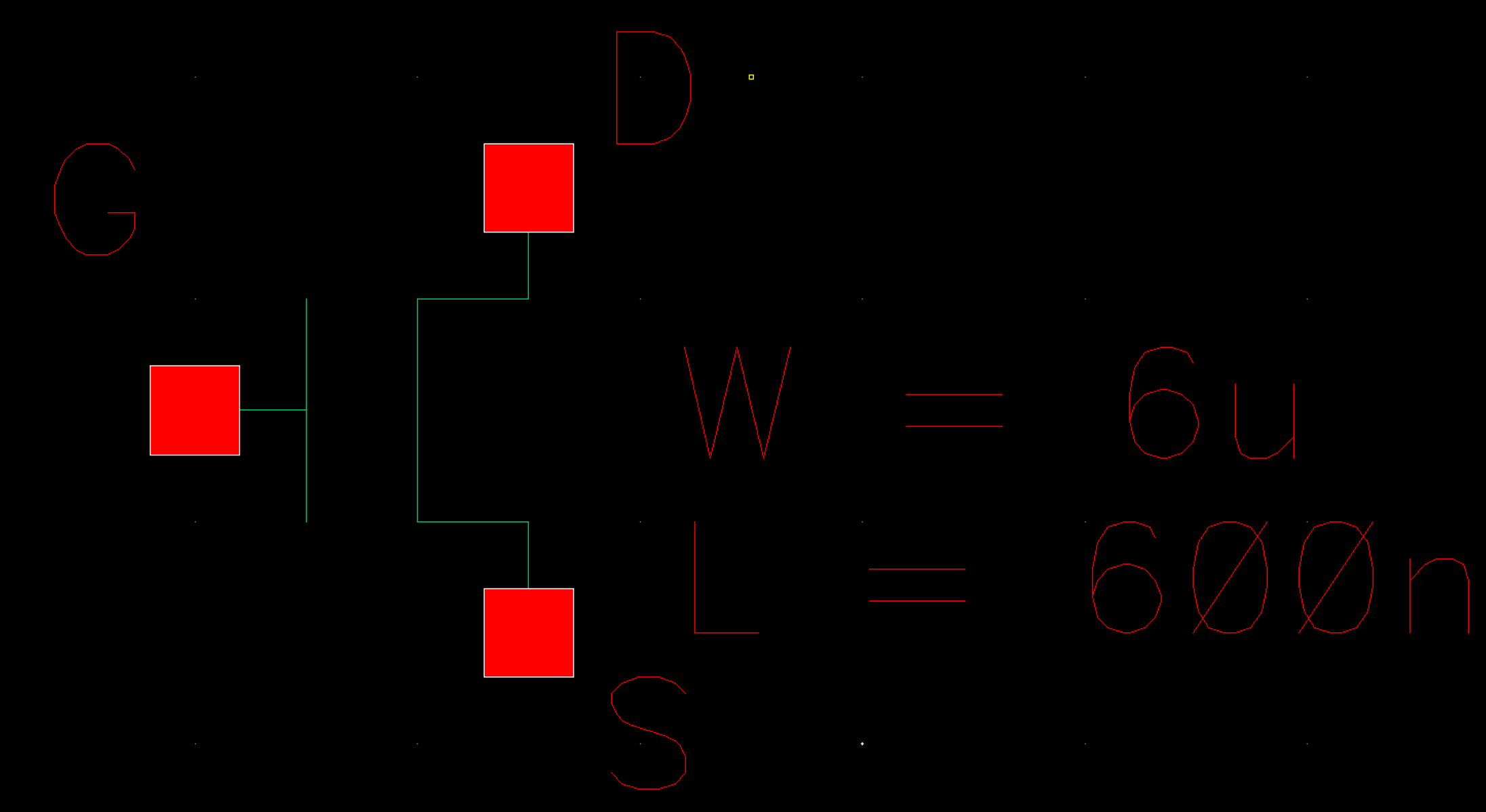
Continuing
on, we created a dedicated 'sim' schematic so we can actually simulate
our NMOS schematic. We made sure to rename V1 to Vds in contrast to
Tutorial 2.
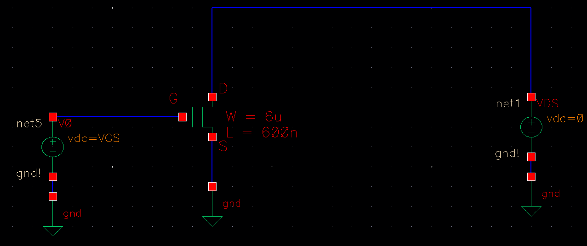
In order to undergo a simulation of our NMOS schematic, we had to add the 'ami06N.m' model library (as seen below).
In
our ADE L window, we made sure we added a 'VGS = 0' design variable,
and the output of the 'D' pin, or Drain, for the current. 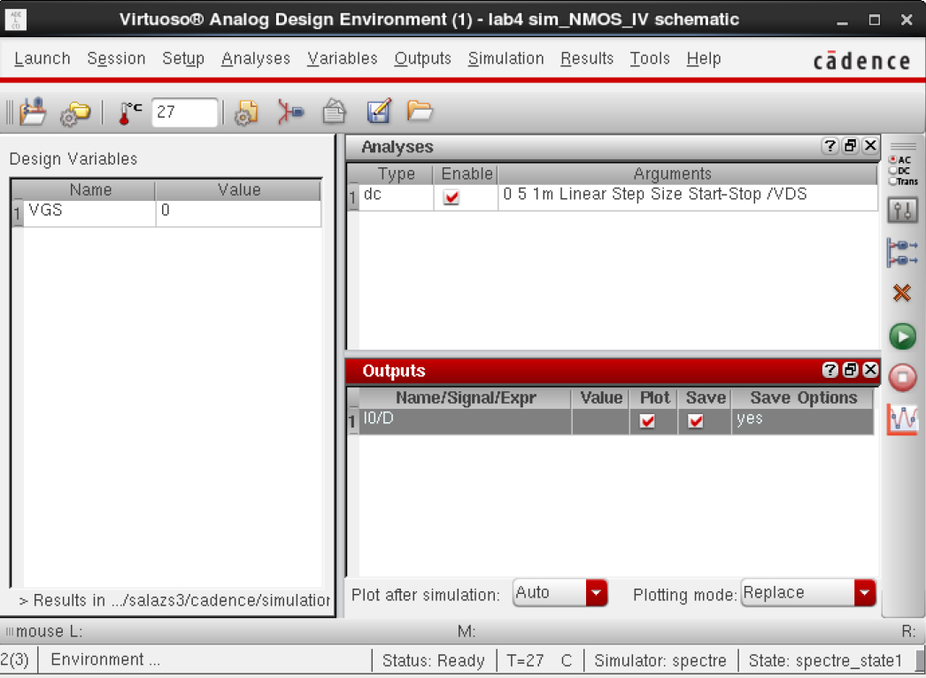
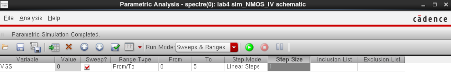
Finally,
we made sure to create a parametric analysis for 'VGS' for a sweep from
0 to 5, and a step mode of 'linear steps' with a step size of '1'.
Here is our simulation results that show the IV curve of our NMOS.
NMOS (ID v. VGS)
In this part of lab 4, we are modifying our NMOS transistor by focusing on a simulation of ID v. VGS.
- VDS is set to 100mV
- VGS is swept from 0 to 2V with 2mV steps
- A DC analysis is undergone ONLY
This was the ADE L dc. analysis with the output of the 'D' pin drain.
Here is our simulation results where the VGS does not start increasing until after the threshhold voltage of about 0.65V.
PMOS (ID v. VSD)
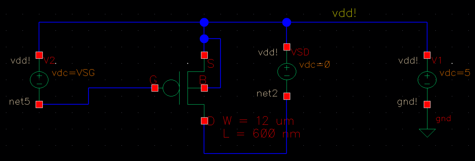
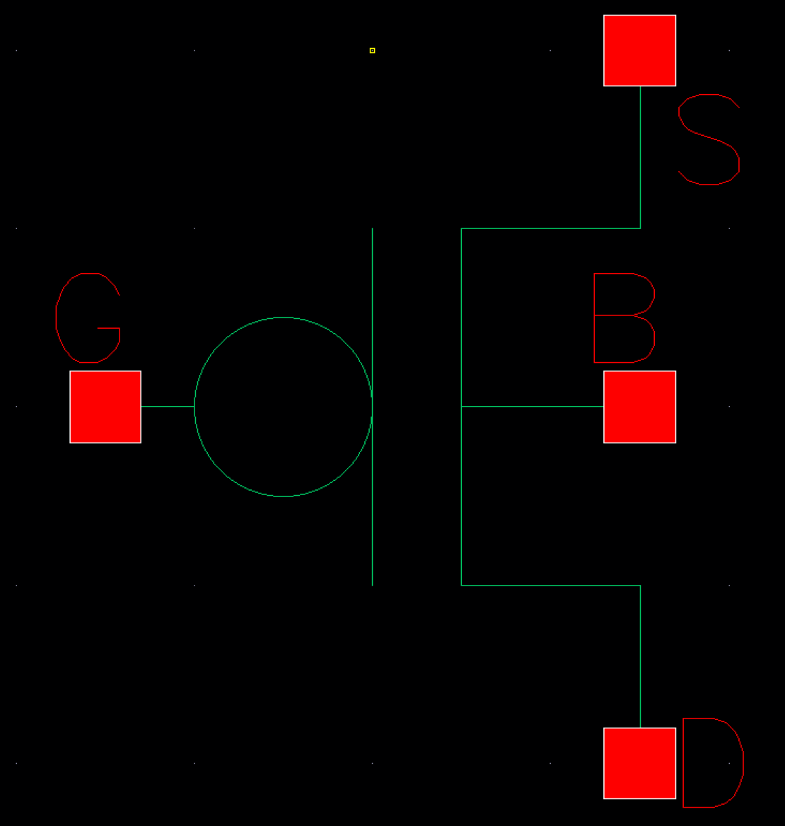
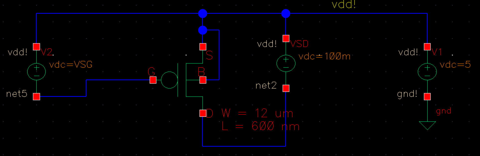
Below is our PMOS schematic with a VDD of 5V and its accompanying symbol with the drain and source
flipped in location compared with the NMOS symbol.
In comparison to the NMOS simulations, we must...
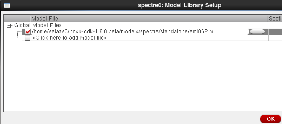
- Use the 'ami06P.m' model library file when undergoing simulations for our PMOS
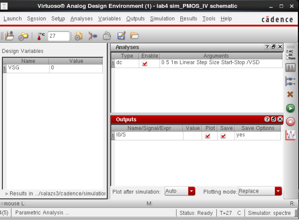
- Undergo a DC analysis in ADE L of 'VSD' with a sweep range from 0 to 5V and a linear step size of 1mV
- Add a variable named 'VSG' in ADE L
- We will do a parametric analyis on 'VSG' from 0 to 5V at 1V linear steps
This is the verification of our correct 'ami06P.m'' model library
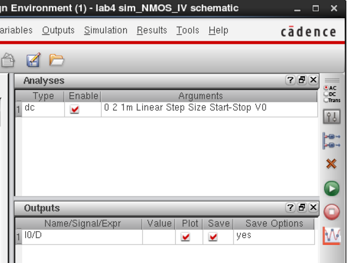
This is the DC analysis settings in ADE L.
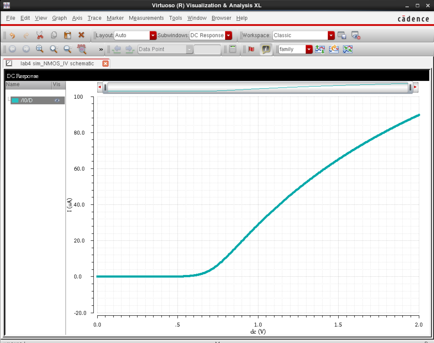
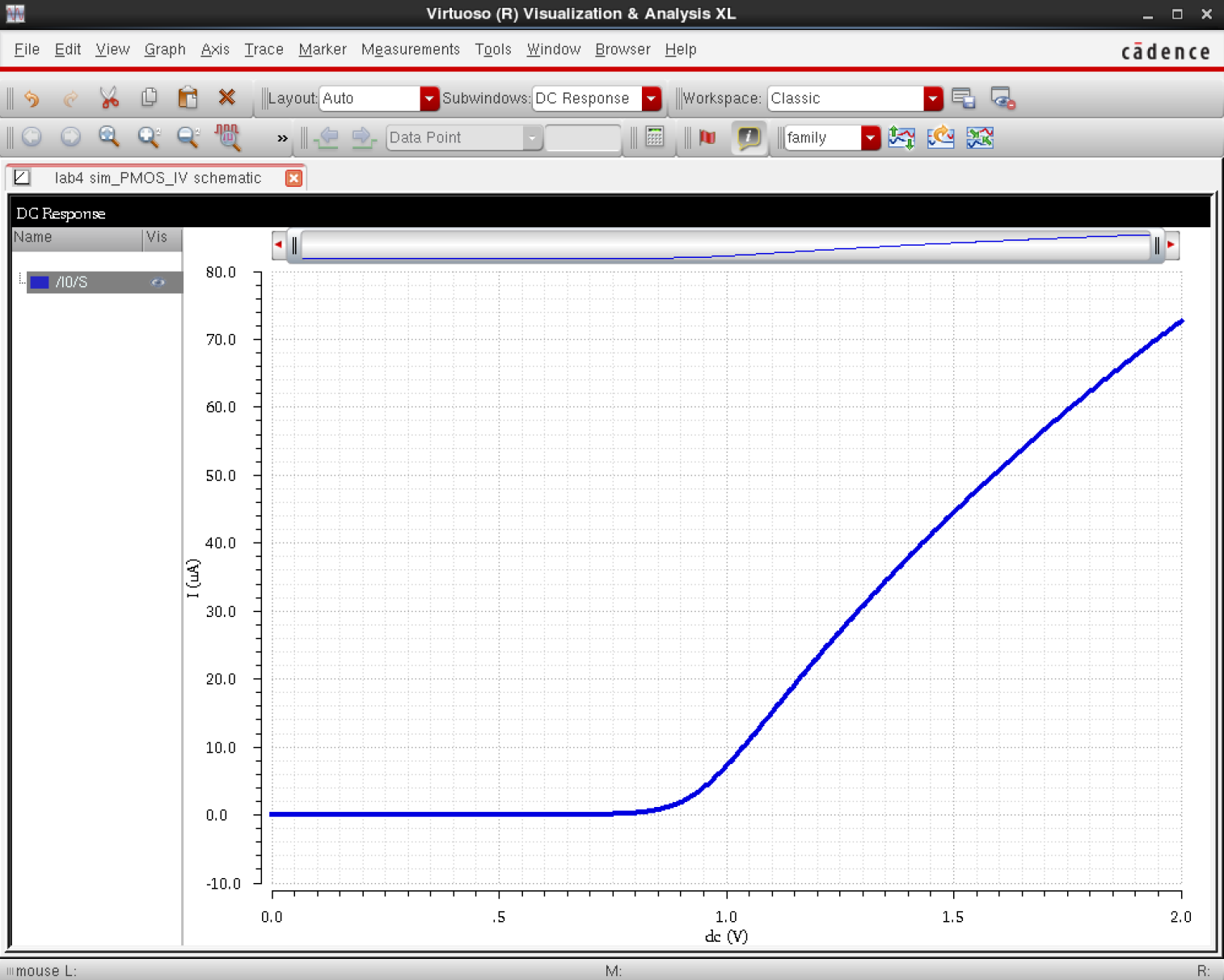
These are our simulation results which resemble the ID v. VDS curve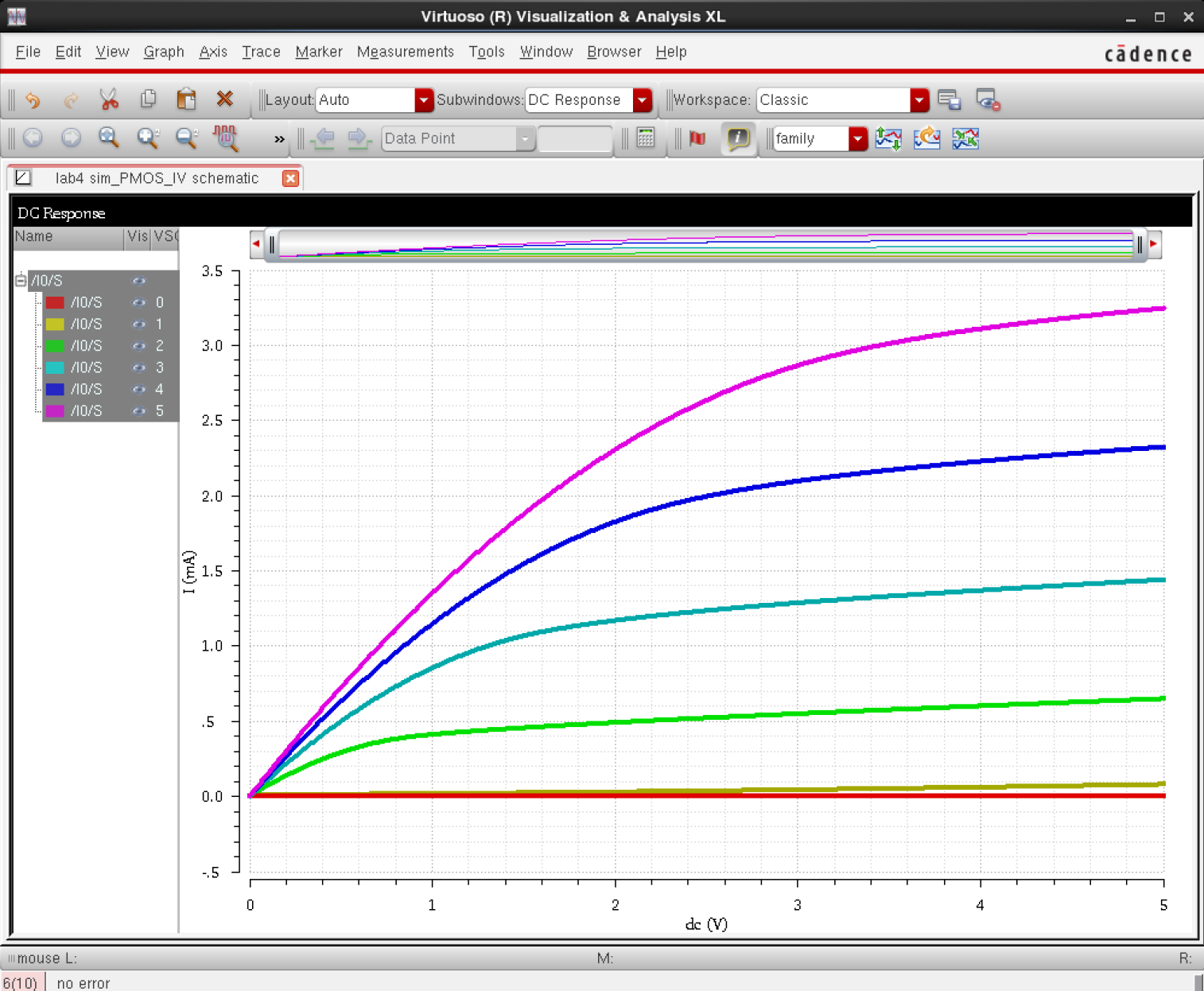
Second PMOS (ID v. VSG)
In this iteration of our PMOS analysis, we are analyzing an ID v. VSG curve with...
- VSD = 100 mV and sweeping from 0 to 2V with 1mV linear step size
- VSG is again swept
- ONLY DC analysis
Verifying our DC Analysis
Simulation results of our ID v. VSG curve with a higher threshold voltage compared to our ID v. VGS curve
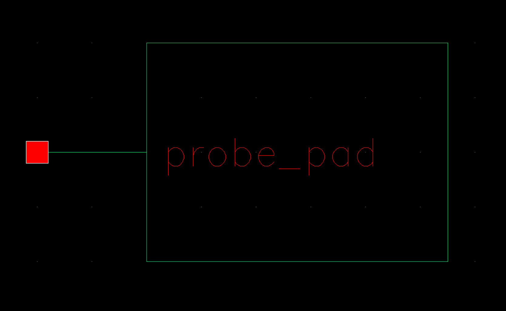
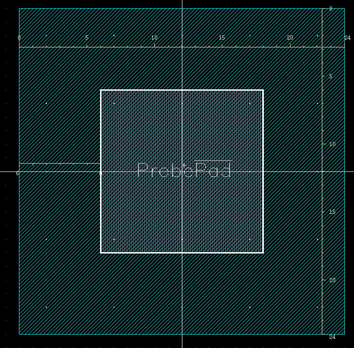
Continuing on with our lab 4, we created a probe pad that will be instantiated later that is 24 u by 24 u in dimensions.
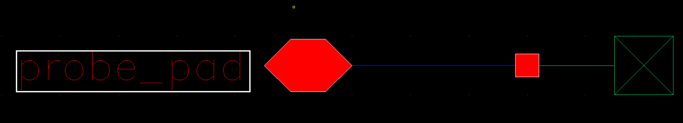
Schematic
of our probe pad
Symbol of our probe pad
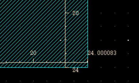
Here
is our probe pad layout that has a metal 3 layer and a glass layer and
the accompanying verification of its correct dimensions below.
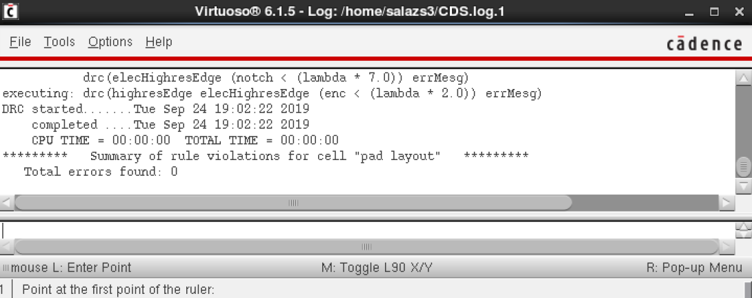
DRC went well...
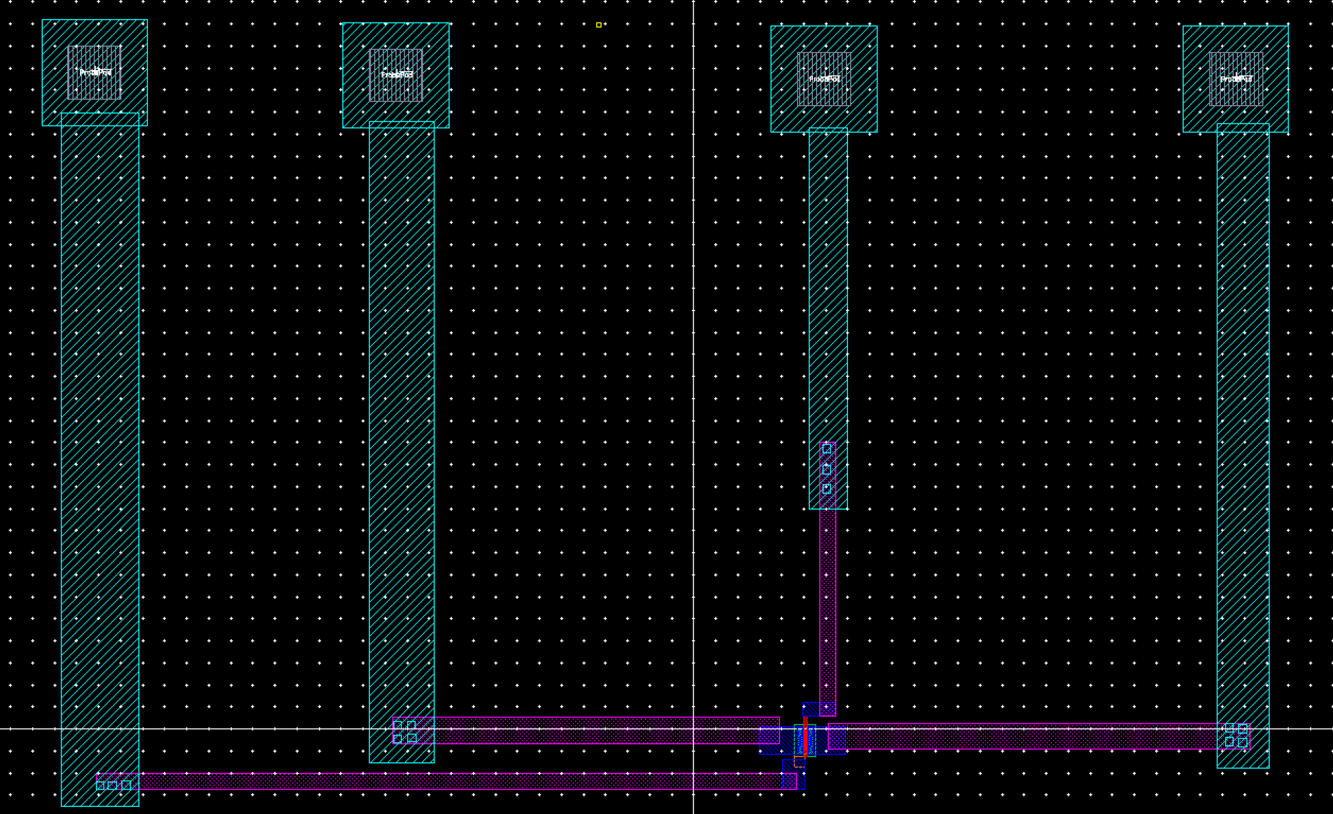
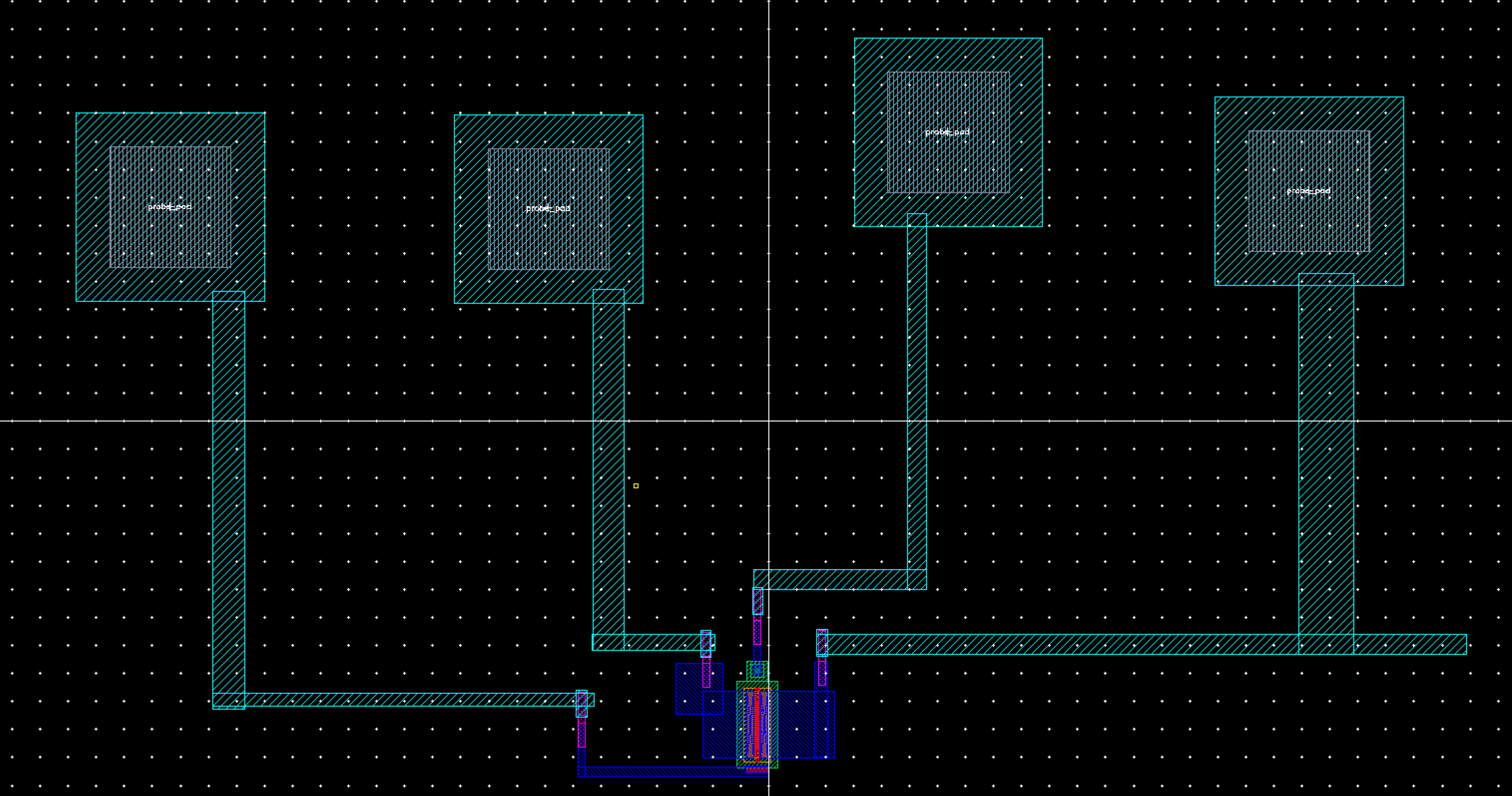
NMOS Pad Layout
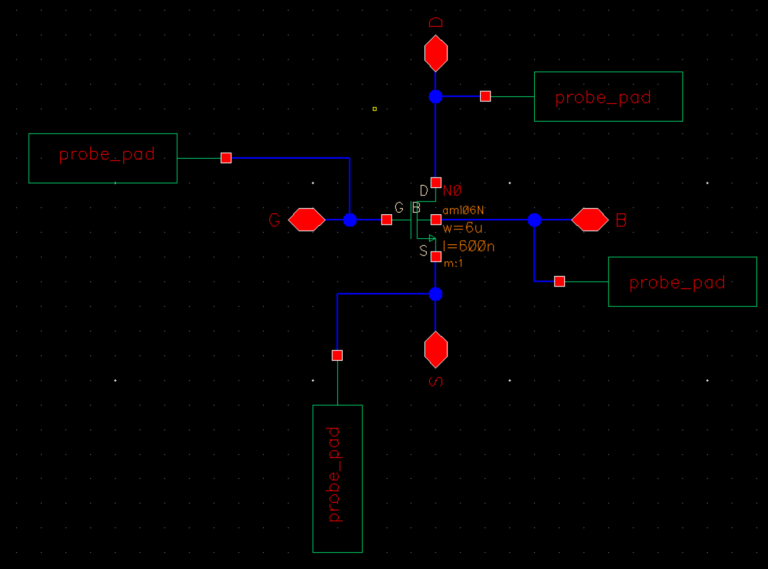
We
created an NMOS transistor (6u/600n) coupled with corresponding probe
pads. Below are its schematic and its corresponding pad layout.
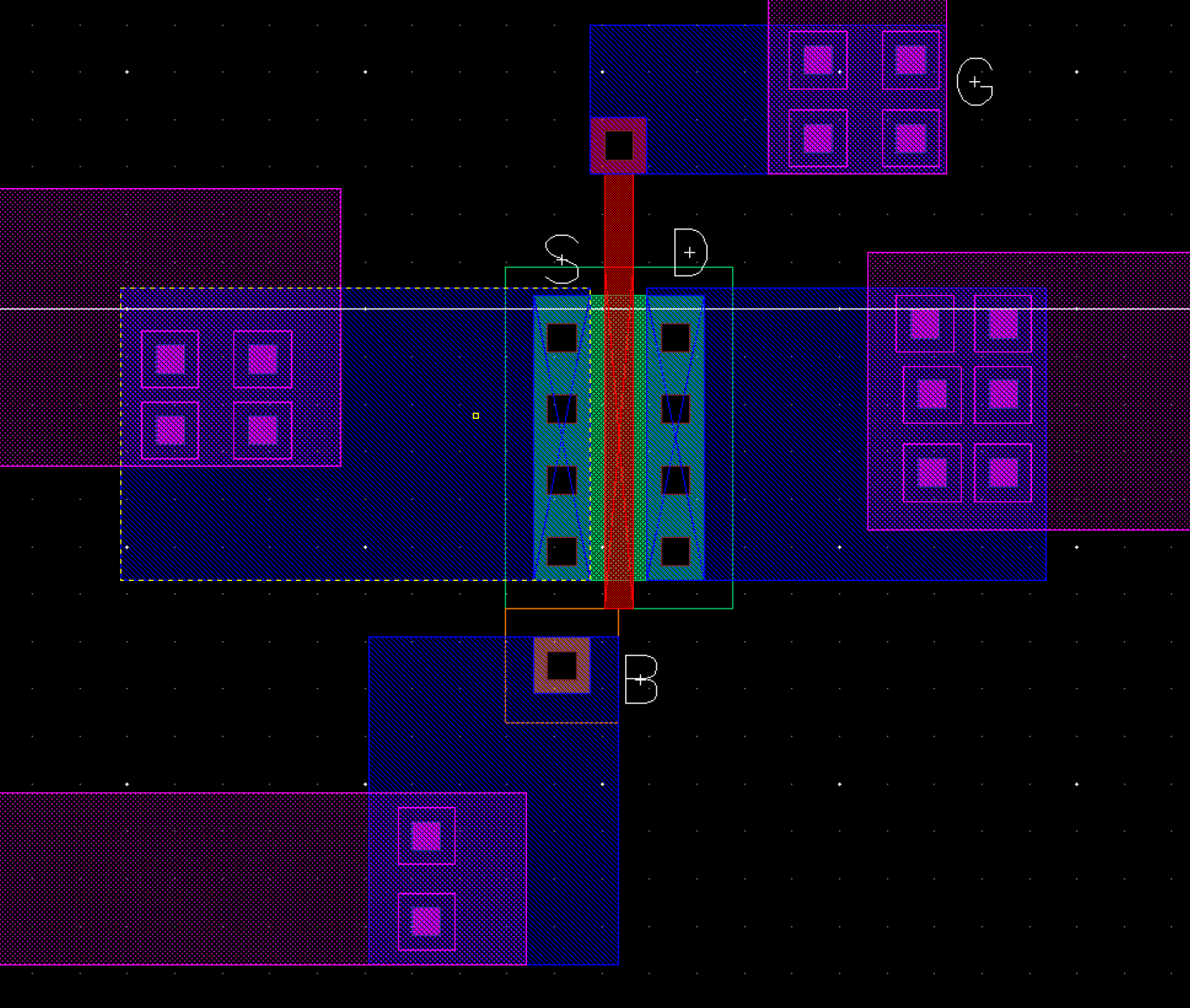
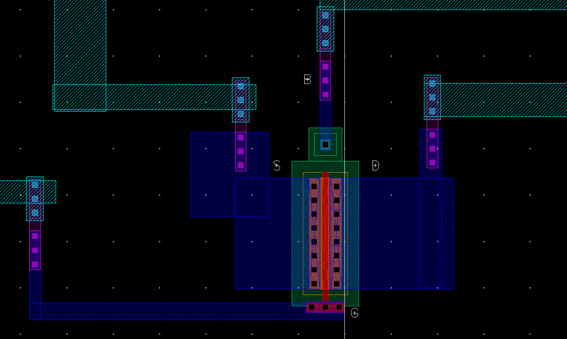
This view gives us a zoomed in view of our NMOS...
- Metal 1 layers from the NMOS are connected with via (m2_m1) to the metal 2 layer
- Metal 2 layers are then connected to Metal 3 layers with via (m3_m2)
- Poly layer is connected with a via (m1_poly) to Metal 1
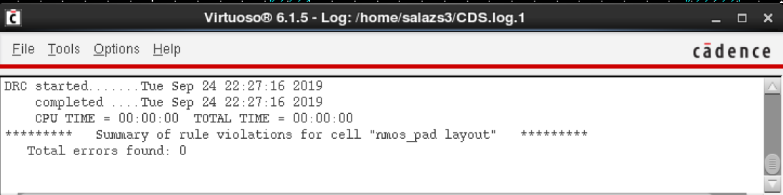
Our NMOS pad layout undergoes DRC nicely...
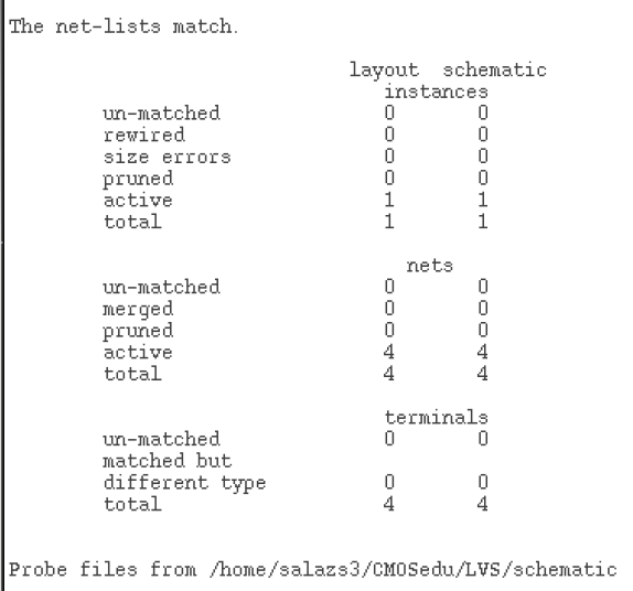
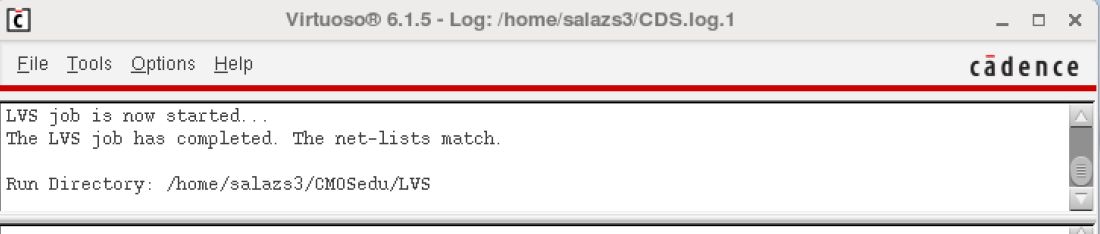
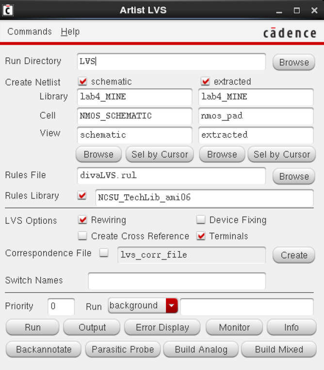
And our NMOS pad layout undergoes LVS nicely as well with the net lists matching...
Switching gears to our PMOS pad layout...
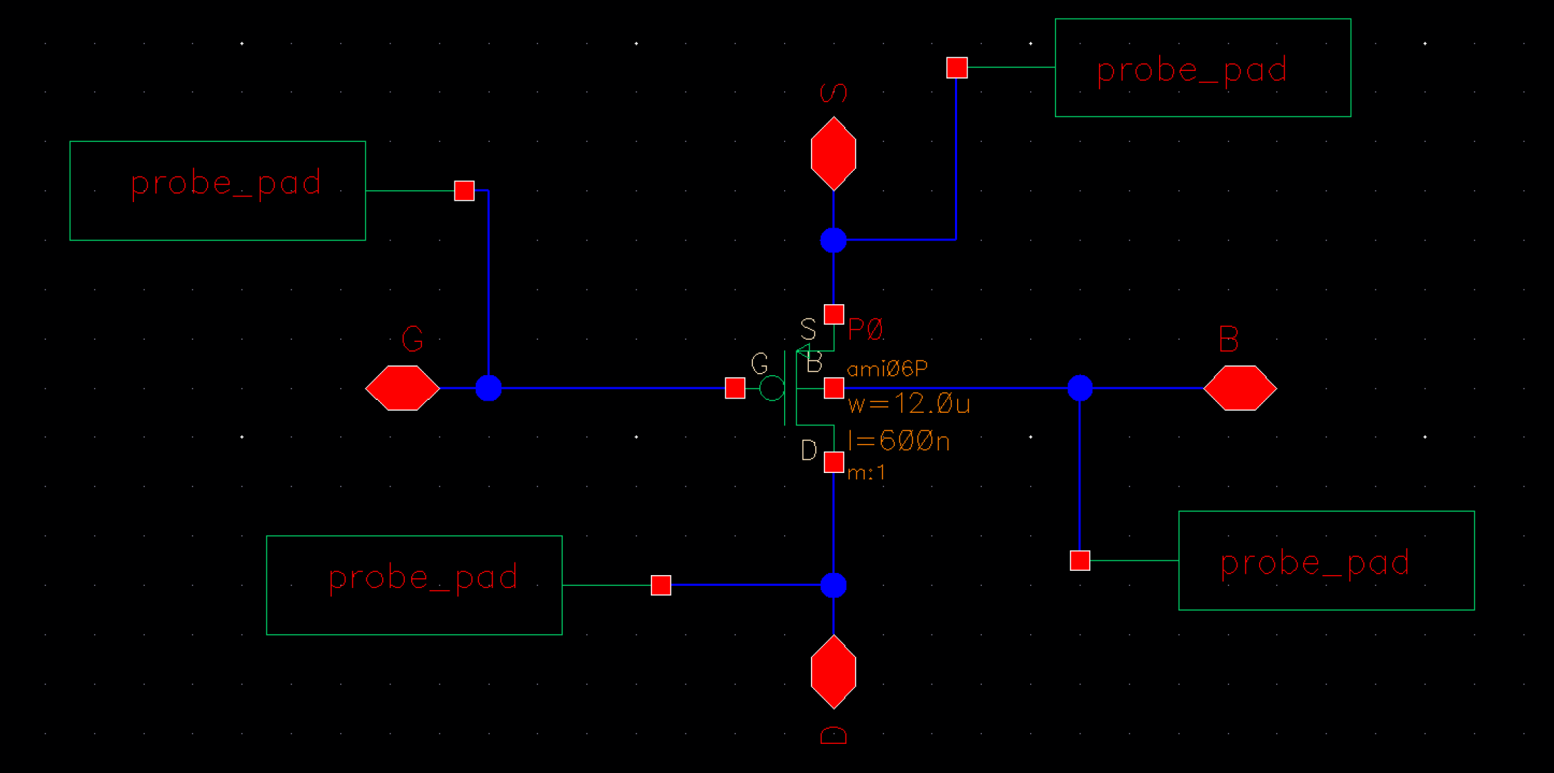
We utilized our PMOS transistor and connected it to our corresponding probe pads as seen below in our layout view.
Below we can see the interconnection of our PMOS transistor to the corresponding pads...
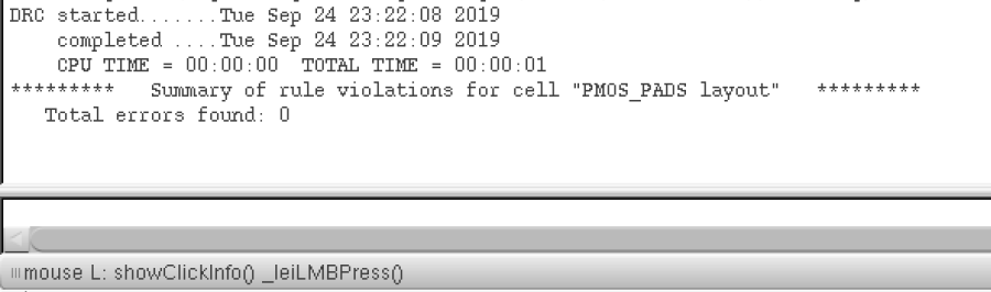
Our PMOS probe pad layout undergoes DRC successfully...
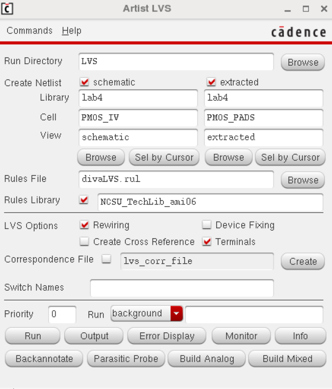
In order to undergo LVS, we made sure to have a proper schematic of our PMOS pad layout (as seen below)...
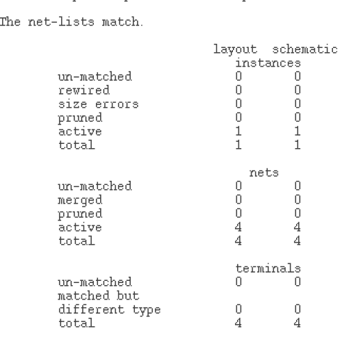
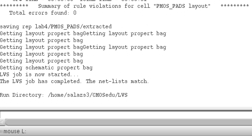
Our PMOS probe pad also undergoes LVS with no errors (net lists match)...
Return to salazs3
Return to EE 421L Labs