Lab 5 - ECE 421L
Authored
by Geovanni Portillo,
Sept 24, 2019
Design, layout, and simulation of a CMOS inverter
All images can be clicked to view the original image
Prelab:
Back-up all of your work from the lab and the course.

Go through Tutorial 3 seen here.
| Inverter Schematic | Inverter Symbol | Inverter Layout | Inverter Extraction |
 |  |  |  |
Showing netlists of schematic and layout match in LVS


Schematic for simulating the inverter

Simulation plot and netlist showing it is an extracted view

Lab:
- Draft schematics, layouts, and symbols for two inverters having sizes of:
- 12u/6u (= width of the PMOS / width of the NMOS with both devices having minimum lengths of 0.6u)
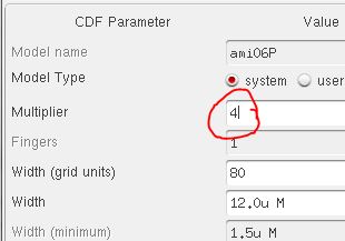
- 48u/24u where the devices use a multiplier, M = 4 (set along with the width and length of the MOSFET, image)
For inverter of widths 12u/6u (pmos/nmos),
Comparing the schematic and extracted view of the layout, we can see the netlists match

For 48u/24u,
Comparing the schematic and extracted view of the layout, we can see the netlists match

The files for the layouts and schematics can be found here
- Using SPICE simulate the operation of both of your inverters showing each driving a 100 fF, 1 pF, 10 pF, and 100 pF capacitive load
- Between the two inverters, the 12u/6u has longer rise/fall times but as the capacitances increase, so do the charging times.
- Use UltraSim (Cadence's fast SPICE simulator for larger circuits at the cost of accuracy) and repeat the above simulations
- There are minor differences in the output plots but the main difference was that the UltraSim simulations were quicker.
| 12u/6u Inverter |
| Capacitance | Schematic | Spectre Output | UltraSim Output |
| 100 fF |  |  |  |
| 1 pF |  |  |  |
| 10 pF |  |  |  |
| 100 pF |  |  |  |
| 48u/24u Inverter |
| Capacitance | Schematic | Spectre Output | UltraSim Output |
| 100 fF |  |  |  |
| 1 pF |  |  |  |
| 10 pF |  |  |  |
| 100 pF |  |  |  |
Reports and Design Libraries are backed up

Return to EE 421 Labs


